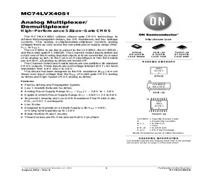
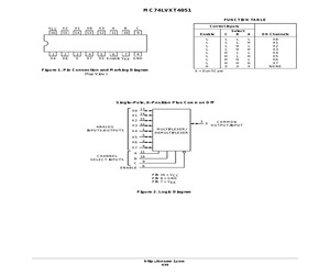
16 VEE VCC A A OFF NC VCC COMMON O/I OFF VEE VEE 6 7 8 Figure 5. Maximum Off Channel Leakage Current, Any One Channel, Test Set-Up HP4195A Network Anl S1 R1 T1 6 7 8 Figure 6. Maximum On Channel Leakage Current, Channel to Channel, Test Set-Up 0.1 F VIS HP11667B Pwr Splitter VCC 100 K 0.1 F ON All untested Analog I/O pins OFF 50 K VEE 6 7 8 N/C COMMON O/I ANALOG I/O VIL VIH VCC ON VEE OFF VCC 16 A 9 - 11 Channel Selects connected to address pins on HP4195A and appropriately configured to test each switch. Figure 7. Maximum On Channel Bandwidth, Test Set-Up http://onsemi.com 6 MC74LVX4051 HP4195A Network Anl S1 R1 T1 0.1 F HP11667B Pwr Splitter 0.1 F VIS VCC 100 K 16 OFF All untested Analog I/O pins ON 50 K VEE 6 7 8 Channel Selects connected to address pins on HP4195A and appropriately configured to test each switch. 9 - 11 Config = Network Format = T/R (dB) CAL = Trans Cal VISO(dB) = 20 log (VT1/VR1) Display = Rectan X*A)B Scale Ref = Auto Scale View = Off, Off, Off Trig = Cont Mode
 16 Pages, 161 KB, Original
16 VEE VCC A A OFF NC VCC COMMON O/I OFF VEE VEE 6 7 8 Figure 5. Maximum Off Channel Leakage Current, Any One Channel, Test Set-Up HP4195A Network Anl S1 R1 T1 6 7 8 Figure 6. Maximum On Channel Leakage Current, Channel to Channel, Test Set-Up 0.1 F VIS HP11667B Pwr Splitter VCC 100 K 0.1 F ON All untested Analog I/O pins OFF 50 K VEE 6 7 8 N/C COMMON O/I ANALOG I/O VIL VIH VCC ON VEE OFF VCC 16 A 9 - 11 Channel Selects connected to address pins on HP4195A and appropriately configured to test each switch. Figure 7. Maximum On Channel Bandwidth, Test Set-Up http://onsemi.com 443 MC74LVXT4051 HP4195A Network Anl S1 R1 T1 0.1 F HP11667B Pwr Splitter 0.1 F VIS 100 K VCC 16 OFF All untested Analog I/O pins ON 50 K VEE 6 7 8 Channel Selects connected to address pins on HP4195A and appropriately configured to test each switch. 9 - 11 Config = Network Format = T/R (dB) CAL = Trans Cal VISO(dB) = 20 log (VT1/VR1) Display = Rectan XAB Scale Ref = Auto Scale View = Off, Off, Off Trig = Cont Mod
 12 Pages, 149 KB, Original
EE VIH Figure 4. Maximum Off Channel Leakage Current, Common Channel, Test Set-Up HP4195A Network Anl S1 R1 T1 16 A VCC COMMON O/I 6 7 8 VEE Figure 3. Maximum Off Channel Leakage Current, Any One Channel, Test Set-Up VCC OFF VCC COMMON O/I VCC 0.1 F VIS HP11667B Pwr Splitter VCC 100 K ON VEE VCC OFF N/C COMMON O/I 0.1 F ON All untested Analog I/O pins ANALOG I/O OFF 50 K VIL VEE 6 7 8 VEE Figure 5. Maximum On Channel Leakage Current, Channel to Channel, Test Set-Up 6 7 8 9 - 11 Channel Selects configured appropriate to test each switch and connected to address pins on HP4195A Figure 6. Maximum On Channel Bandwidth, Test Set-Up http://onsemi.com 8 MC74LVX4052 HP4195A Network Anl S1 R1 T1 HP4195A Network Anl S1 R1 T1 0.1 F HP11667B Pwr Splitter VIS 0.1 F VIS HP11667B Pwr Splitter VCC 100 K 0.1 F VCC 100 K 16 0.1 F OFF All untested Analog I/O pins 16 OFF ON 50 K ON 50 K VEE 6 7 8 Config = Network Format = T/R (dB) CAL = Trans Cal Display = Rectan X-A+B Scale Ref = Auto Scal
 16 Pages, 183 KB, Original
Voltage of Enabled Channel due to Injected Current on a Disabled Channel (1-of-4 SPDTs Shown Tested) Figure 8. Power Dissipation Capacitance Test Set-Up (per Channel, 1-of-4 Switching) http://onsemi.com 7 NLAS44599 HP4195A Network Anl S1 R1 T1 0.1 F VIS HP11667B Pwr Splitter 100 K VCC 0.1 F 1 VCC 2 16 15 14 13 4 3 2 1 12 11 10 9 1 50 2 1 8 7 6 5 50 2 Figure 9.Maximum On-Channel Bandwidth Test Set-Up (1 Channel of 1-of-4 SPDTs Shown Tested) HP4195A Network Anl S1 R1 T1 0.1 F VIS HP11667B Pwr Splitter 100 K Config = Network Format = T/R (dB) CAL - Trans Cal Display = Rectan X-A+B Scale Ref = Auto Scale View = Off, Off, Off Trig = Cont Mode Source Amplitude = +13 dB Reference Attenuation = 20 dB Test Attenuation = 0 dB 0.1 F 1 VCC VCC 2 1 12 11 10 9 4 3 2 1 16 15 14 13 50 2 1 50 8 7 6 5 2 Figure 10. Off-Channel Feedthrough Isolation Test Set-Up (1 Channel of 1-of-4 SPDTs Shown Tested) http://onsemi.com 8 NLAS44599 Config = Network Format = T/R (dB) CAL - Trans Cal Display = Rectan X-A+B
 20 Pages, 149 KB, Original
16 VEE VCC A A OFF NC VCC COMMON O/I OFF VEE VEE 6 7 8 Figure 5. Maximum Off Channel Leakage Current, Any One Channel, Test Set-Up HP4195A Network Anl S1 R1 T1 6 7 8 Figure 6. Maximum On Channel Leakage Current, Channel to Channel, Test Set-Up 0.1 F VIS HP11667B Pwr Splitter VCC 100 K 0.1 F ON All untested Analog I/O pins OFF 50 K VEE 6 7 8 N/C COMMON O/I ANALOG I/O VIL VIH VCC ON VEE OFF VCC 16 A 9-1 1 Channel Selects connected to address pins on HP4195A and appropriately configured to test each switch. Figure 7. Maximum On Channel Bandwidth, Test Set-Up http://onsemi.com 6 MC74LVX4053 HP4195A Network Anl S1 R1 T1 0.1 F HP11667B Pwr Splitter 0.1 F VIS VCC 100 K 16 OFF All untested Analog I/O pins ON 50 K VEE 6 7 8 Channel Selects connected to address pins on HP4195A and appropriately configured to test each switch. 9-1 1 Config = Network Format = T/R (dB) CAL = Trans Cal VISO(dB) = 20 log (VT1/VR1) Display = Rectan X*A)B Scale Ref = Auto Scale View = Off, Off, Off Trig = Cont Mode S
 15 Pages, 149 KB, Original
16 VEE VCC A A OFF NC VCC COMMON O/I OFF VEE VEE 6 7 8 Figure 5. Maximum Off Channel Leakage Current, Any One Channel, Test Set-Up HP4195A Network Anl S1 R1 T1 6 7 8 Figure 6. Maximum On Channel Leakage Current, Channel to Channel, Test Set-Up 0.1 F VIS HP11667B Pwr Splitter VCC 100 K 0.1 F ON All untested Analog I/O pins OFF 50 K VEE 6 7 8 N/C COMMON O/I ANALOG I/O VIL VIH VCC ON VEE OFF VCC 16 A 9 - 11 Channel Selects connected to address pins on HP4195A and appropriately configured to test each switch. Figure 7. Maximum On Channel Bandwidth, Test Set-Up http://onsemi.com 443 MC74LVXT4051 HP4195A Network Anl S1 R1 T1 0.1 F HP11667B Pwr Splitter 0.1 F VIS 100 K VCC 16 OFF All untested Analog I/O pins ON 50 K VEE 6 7 8 Channel Selects connected to address pins on HP4195A and appropriately configured to test each switch. 9 - 11 Config = Network Format = T/R (dB) CAL = Trans Cal VISO(dB) = 20 log (VT1/VR1) Display = Rectan XAB Scale Ref = Auto Scale View = Off, Off, Off Trig = Cont Mod
 11 Pages, 122 KB, Original
EE VIH Figure 4. Maximum Off Channel Leakage Current, Common Channel, Test Set-Up HP4195A Network Anl S1 R1 T1 16 A VCC COMMON O/I 6 7 8 VEE Figure 3. Maximum Off Channel Leakage Current, Any One Channel, Test Set-Up VCC OFF VCC COMMON O/I VCC 0.1 F VIS HP11667B Pwr Splitter VCC 100 K ON VEE VCC OFF N/C COMMON O/I 0.1 F ON All untested Analog I/O pins ANALOG I/O OFF 50 K VIL VEE 6 7 8 VEE Figure 5. Maximum On Channel Leakage Current, Channel to Channel, Test Set-Up 6 7 8 9 - 11 Channel Selects configured appropriate to test each switch and connected to address pins on HP4195A Figure 6. Maximum On Channel Bandwidth, Test Set-Up http://onsemi.com 8 MC74LVX4053 HP4195A Network Anl S1 R1 T1 HP4195A Network Anl S1 R1 T1 0.1 F HP11667B Pwr Splitter VIS 0.1 F VIS HP11667B Pwr Splitter VCC 100 K 0.1 F VCC 100 K 16 0.1 F OFF All untested Analog I/O pins 16 OFF ON 50 K ON 50 K VEE 6 7 8 Config = Network Format = T/R (dB) CAL = Trans Cal Display = Rectan X-A+B Scale Ref = Auto Scal
 16 Pages, 197 KB, Original
16 VEE VCC A A OFF NC VCC COMMON O/I OFF VEE VEE 6 7 8 Figure 5. Maximum Off Channel Leakage Current, Any One Channel, Test Set-Up HP4195A Network Anl S1 R1 T1 6 7 8 Figure 6. Maximum On Channel Leakage Current, Channel to Channel, Test Set-Up 0.1 F VIS HP11667B Pwr Splitter VCC 100 K 0.1 F ON All untested Analog I/O pins OFF 50 K VEE 6 7 8 N/C COMMON O/I ANALOG I/O VIL VIH VCC ON VEE OFF VCC 16 A 9 - 11 Channel Selects connected to address pins on HP4195A and appropriately configured to test each switch. Figure 7. Maximum On Channel Bandwidth, Test Set-Up http://onsemi.com 6 MC74LVXT4052 HP4195A Network Anl S1 R1 T1 0.1 F HP11667B Pwr Splitter 0.1 F VIS VCC 100 K 16 OFF All untested Analog I/O pins ON 50 K VEE 6 7 8 Channel Selects connected to address pins on HP4195A and appropriately configured to test each switch. 9 - 11 Config = Network Format = T/R (dB) CAL = Trans Cal VISO(dB) = 20 log (VT1/VR1) Display = Rectan XAB Scale Ref = Auto Scale View = Off, Off, Off Trig = Cont Mode
 16 Pages, 144 KB, Original
 ON VEE OFF NC 16 A A VCC COMMON O/I OFF VEE VEE 6 7 8 Figure 5. Maximum Off Channel Leakage Current, Any One Channel, Test Set-Up HP4195A Network Anl S1 R1 T1 6 7 8 Figure 6. Maximum On Channel Leakage Current, Channel to Channel, Test Set-Up 0.1 F VIS HP11667B Pwr Splitter VCC 100 K 0.1 F ON All untested Analog I/O pins OFF 50 K VEE 6 7 8 N/C COMMON O/I ANALOG I/O VIL VIH VCC 9 - 11 Channel Selects connected to address pins on HP4195A and appropriately configured to test each switch. Figure 7. Maximum On Channel Bandwidth, Test Set-Up http://onsemi.com 6 MC74LVX4051 HP4195A Network Anl S1 R1 T1 0.1 F HP11667B Pwr Splitter 0.1 F VIS VCC 100 K 16 OFF All untested Analog I/O pins ON 50 K VEE 6 7 8 Channel Selects connected to address pins on HP4195A and appropriately configured to test each switch. 9 - 11 Config = Network Format = T/R (dB) CAL = Trans Cal VISO(dB) = 20 log (VT1/VR1) Display = Rectan X*A)B Scale Ref = Auto Scale View = Off, Off, Off Trig = Cont Mode Source Amplitude =
 15 Pages, 184 KB, Original
16 VEE VCC A A OFF NC VCC COMMON O/I OFF VEE VEE 6 7 8 Figure 5. Maximum Off Channel Leakage Current, Any One Channel, Test Set-Up HP4195A Network Anl S1 R1 T1 6 7 8 Figure 6. Maximum On Channel Leakage Current, Channel to Channel, Test Set-Up 0.1 F VIS HP11667B Pwr Splitter VCC 100 K 0.1 F ON All untested Analog I/O pins OFF 50 K VEE 6 7 8 N/C COMMON O/I ANALOG I/O VIL VIH VCC ON VEE OFF VCC 16 A 9 - 11 Channel Selects connected to address pins on HP4195A and appropriately configured to test each switch. Figure 7. Maximum On Channel Bandwidth, Test Set-Up http://onsemi.com 6 MC74LVXT4051 HP4195A Network Anl S1 R1 T1 0.1 F HP11667B Pwr Splitter 0.1 F VIS 100 K VCC 16 OFF All untested Analog I/O pins ON 50 K VEE 6 7 8 Channel Selects connected to address pins on HP4195A and appropriately configured to test each switch. 9 - 11 Config = Network Format = T/R (dB) CAL = Trans Cal VISO(dB) = 20 log (VT1/VR1) Display = Rectan XAB Scale Ref = Auto Scale View = Off, Off, Off Trig = Cont Mode
 16 Pages, 142 KB, Original
16 VEE VCC A A OFF NC VCC COMMON O/I OFF VEE VEE 6 7 8 Figure 5. Maximum Off Channel Leakage Current, Any One Channel, Test Set-Up HP4195A Network Anl S1 R1 T1 6 7 8 Figure 6. Maximum On Channel Leakage Current, Channel to Channel, Test Set-Up 0.1 F VIS HP11667B Pwr Splitter VCC 100 K 0.1 F ON All untested Analog I/O pins OFF 50 K VEE 6 7 8 N/C COMMON O/I ANALOG I/O VIL VIH VCC ON VEE OFF VCC 16 A 9 - 11 Channel Selects connected to address pins on HP4195A and appropriately configured to test each switch. Figure 7. Maximum On Channel Bandwidth, Test Set-Up http://onsemi.com 6 MC74LVXT4052 HP4195A Network Anl S1 R1 T1 0.1 F HP11667B Pwr Splitter 0.1 F VIS VCC 100 K 16 OFF All untested Analog I/O pins ON 50 K VEE 6 7 8 Channel Selects connected to address pins on HP4195A and appropriately configured to test each switch. 9 - 11 Config = Network Format = T/R (dB) CAL = Trans Cal VISO(dB) = 20 log (VT1/VR1) Display = Rectan XAB Scale Ref = Auto Scale View = Off, Off, Off Trig = Cont Mode
 16 Pages, 145 KB, Original
4. Maximum Off Channel Leakage Current, Any One Channel, Test Set-Up VCC 16 A VCC ON VEE VCC OFF N/C COMMON O/I ANALOG I/O VIL 6 7 8 VEE Figure 5. Maximum On Channel Leakage Current, Channel to Channel, Test Set-Up HP4195A Network Anl S1 R1 T1 0.1 F VIS HP11667B Pwr Splitter VCC 100 K 0.1 F ON All untested Analog I/O pins OFF 50 K VEE 6 7 8 9 - 11 Channel Selects connected to address pins on HP4195A and appropriately configured to test each switch. Figure 6. Maximum On Channel Bandwidth, Test Set-Up http://onsemi.com 6 MC74LVX4052 HP4195A Network Anl S1 R1 T1 0.1 F HP11667B Pwr Splitter 0.1 F VIS VCC 100 K 16 OFF All untested Analog I/O pins ON 50 K VEE 6 7 8 Channel Selects connected to address pins on HP4195A and appropriately configured to test each switch. 9 - 11 Config = Network Format = T/R (dB) CAL = Trans Cal VISO(dB) = 20 log (VT1/VR1) Display = Rectan X*A)B Scale Ref = Auto Scale View = Off, Off, Off Trig = Cont Mode Source Amplitude = )13 dB Reference Attenuation = 20 dB T
 15 Pages, 258 KB, Original
16 VEE VCC A A OFF NC VCC COMMON O/I OFF VEE VEE 6 7 8 Figure 5. Maximum Off Channel Leakage Current, Any One Channel, Test Set-Up HP4195A Network Anl S1 R1 T1 6 7 8 Figure 6. Maximum On Channel Leakage Current, Channel to Channel, Test Set-Up 0.1 F VIS HP11667B Pwr Splitter VCC 100 K 0.1 F ON All untested Analog I/O pins OFF 50 K VEE 6 7 8 N/C COMMON O/I ANALOG I/O VIL VIH VCC ON VEE OFF VCC 16 A 9 - 11 Channel Selects connected to address pins on HP4195A and appropriately configured to test each switch. Figure 7. Maximum On Channel Bandwidth, Test Set-Up http://onsemi.com 6 MC74LVXT4052 HP4195A Network Anl S1 R1 T1 0.1 F HP11667B Pwr Splitter 0.1 F VIS 100 K VCC 16 OFF All untested Analog I/O pins ON 50 K VEE 6 7 8 Channel Selects connected to address pins on HP4195A and appropriately configured to test each switch. 9 - 11 Config = Network Format = T/R (dB) CAL = Trans Cal VISO(dB) = 20 log (VT1/VR1) Display = Rectan XAB Scale Ref = Auto Scale View = Off, Off, Off Trig = Cont Mode
 16 Pages, 142 KB, Original
16 VEE VCC A A OFF NC VCC COMMON O/I OFF VEE VEE 6 7 8 Figure 5. Maximum Off Channel Leakage Current, Any One Channel, Test Set-Up HP4195A Network Anl S1 R1 T1 6 7 8 Figure 6. Maximum On Channel Leakage Current, Channel to Channel, Test Set-Up 0.1 F VIS HP11667B Pwr Splitter VCC 100 K 0.1 F ON All untested Analog I/O pins OFF 50 K VEE 6 7 8 N/C COMMON O/I ANALOG I/O VIL VIH VCC ON VEE OFF VCC 16 A 9 - 11 Channel Selects connected to address pins on HP4195A and appropriately configured to test each switch. Figure 7. Maximum On Channel Bandwidth, Test Set-Up http://onsemi.com 99 MC74LVX4051 HP4195A Network Anl S1 R1 T1 0.1 F HP11667B Pwr Splitter 0.1 F VIS 100 K VCC 16 OFF All untested Analog I/O pins ON 50 K VEE 6 7 8 Channel Selects connected to address pins on HP4195A and appropriately configured to test each switch. 9 - 11 Config = Network Format = T/R (dB) CAL = Trans Cal VISO(dB) = 20 log (VT1/VR1) Display = Rectan XAB Scale Ref = Auto Scale View = Off, Off, Off Trig = Cont Mode
 12 Pages, 132 KB, Original
16 VEE VCC A A OFF NC VCC COMMON O/I OFF VEE VEE 6 7 8 Figure 5. Maximum Off Channel Leakage Current, Any One Channel, Test Set-Up HP4195A Network Anl S1 R1 T1 6 7 8 Figure 6. Maximum On Channel Leakage Current, Channel to Channel, Test Set-Up 0.1 F VIS HP11667B Pwr Splitter VCC 100 K 0.1 F ON All untested Analog I/O pins OFF 50 K VEE 6 7 8 N/C COMMON O/I ANALOG I/O VIL VIH VCC ON VEE OFF VCC 16 A 9 - 11 Channel Selects connected to address pins on HP4195A and appropriately configured to test each switch. Figure 7. Maximum On Channel Bandwidth, Test Set-Up http://onsemi.com 491 MC74LVXT4053 HP4195A Network Anl S1 R1 T1 0.1 F HP11667B Pwr Splitter 0.1 F VIS 100 K VCC 16 OFF All untested Analog I/O pins ON 50 K VEE 6 7 8 Channel Selects connected to address pins on HP4195A and appropriately configured to test each switch. 9 - 11 Config = Network Format = T/R (dB) CAL = Trans Cal VISO(dB) = 20 log (VT1/VR1) Display = Rectan XAB Scale Ref = Auto Scale View = Off, Off, Off Trig = Cont Mod
 12 Pages, 146 KB, Original


