2M DF04M FUF4005 FUF4006 FUF4007 DF06M FUF4005 FUF4005 W10F W01F W02F W04F W005F W06F W08F BZX85C110GP BZX85C120GP BZX85C120GP BZX85C130GP BZX85C130GP BZX85C150GP BZX85C150GP BZX85C160GP BZX85C160GP BZX85C180GP BZX85C180GP BZX85C200GP BZX85C200GP 1N4003GP 1N4004GP 1N4005GP 1N4006GP 1N4007GP 1N4001GP 1N4001GP 1N4001GP 1N4001GP 1N4001GP 1N4001GP 1N4001GP 1N4001GP 1N4001GP 1N4001GP 1N4001GP 1N4001GP 1N4001GP 1N4001GP 1N4001GP 922 Cross Reference Competitor Part Number Competitor FAGOR Part Number Competitor Part Number Competitor FAGOR Part Number 1N4001GP 1N4001ID 1N4002 1N4002 1N4002 1N4002 1N4002 1N4002 1N4002 1N4002 1N4002 1N4002G 1N4002G 1N4002G 1N4002G 1N4002G 1N4002G 1N4002GP 1N4002ID 1N4003 1N4003 1N4003 1N4003 1N4003 1N4003 1N4003 1N4003 1N4003 1N4003G 1N4003G 1N4003G 1N4003G 1N4003G 1N4003GP 1N4003ID 1N4004 1N4004 1N4004 1N4004 1N4004 1N4004 1N4004 1N4004 1N4004 1N4004G 1N4004G 1N4004G 1N4004G 1N4004G 1N4004G 1N4004GP 1N4004ID 1N4005 VISHAY PHILIPS DIOTEC PANJIT TSC ON Semicon
 136 Pages, 7525 KB, Original
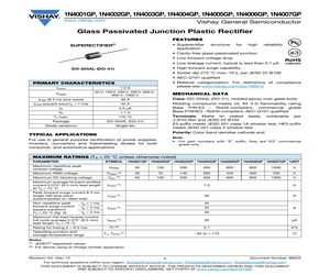
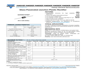
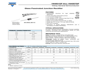
1N4004GP, 1N4005GP, 1N4006GP, 1N4007GP www.vishay.com Vishay General Semiconductor Glass Passivated Junction Plastic Rectifier FEATURES * Superectifier application SUPERECTIFIER(R) structure for high reliability * Cavity-free glass-passivated junction * Low forward voltage drop * Low leakage current, typical IR less than 0.1 A * High forward surge capability * Solder dip 275 C max. 10 s, per JESD 22-B106 DO-204AL (DO-41) * Material categorization: for definitions of compliance please see www.vishay.com/doc?99912 TYPICAL APPLICATIONS For use in general purpose rectification of power supplies, inverters, converters and freewheeling diodes for consumer applications. PRIMARY CHARACTERISTICS IF(AV) 1.0 A VRRM 50 V, 100 V, 200 V, 400 V, 600 V, 800 V, 1000 V IFSM (8.3 ms sine-wave) 30 A IFSM (square wave tp = 1 ms) 45 A IR 5.0 A MECHANICAL DATA Case: DO-204AL (DO-41), molded epoxy over glass body Molding compound meets UL 94 V-0 flammability rating Base P/N-E3 - RoHS-compliant, commercial grade VF 1.1 V
 6 Pages, 104 KB, Original
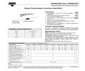
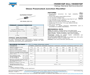
1N4004GP, 1N4005GP, 1N4006GP, 1N4007GP www.vishay.com Vishay General Semiconductor Glass Passivated Junction Plastic Rectifier FEATURES SUPERECTIFIER * Superectifier application (R) structure for high reliability * Cavity-free glass-passivated junction * Low forward voltage drop * Low leakage current, typical IR less than 0.1 A * High forward surge capability DO-204AL (DO-41) * Solder dip 275 C max. 10 s, per JESD 22-B106 * AEC-Q101 qualified * Material categorization: For definitions of compliance please see www.vishay.com/doc?99912 PRIMARY CHARACTERISTICS IF(AV) 1.0 A VRRM 50 V, 100 V, 200 V, 400 V, 600 V, 800 V, 1000 V MECHANICAL DATA IFSM (8.3 ms sine-wave) 30 A Case: DO-204AL (DO-41), molded epoxy over glass body IFSM (square wave tp = 1 ms) 45 A IR 5.0 A VF 1.1 V Molding compound meets UL 94 V-0 flammability rating Base P/N-E3 - RoHS-compliant, commercial grade Base P/NHE3 - RoHS-compliant, AEC-Q101 qualified TJ max. 175 C Package DO-204AL (DO-41) Diode variations Single die Terminals: Matt
 5 Pages, 74 KB, Original
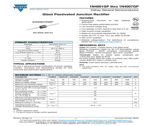
1N4004GP, 1N4005GP, 1N4006GP, 1N4007GP www.vishay.com Vishay General Semiconductor Glass Passivated Junction Plastic Rectifier FEATURES SUPERECTIFIER * Superectifier application (R) structure for high reliability * Cavity-free glass-passivated junction * Low forward voltage drop * Low leakage current, typical IR less than 0.1 A * High forward surge capability DO-204AL (DO-41) * Solder dip 275 C max. 10 s, per JESD 22-B106 * AEC-Q101 qualified * Material categorization: For definitions of compliance please see www.vishay.com/doc?99912 PRIMARY CHARACTERISTICS IF(AV) 1.0 A VRRM 50 V, 100 V, 200 V, 400 V, 600 V, 800 V, 1000 V MECHANICAL DATA IFSM (8.3 ms sine-wave) 30 A Case: DO-204AL (DO-41), molded epoxy over glass body IFSM (square wave tp = 1 ms) 45 A IR 5.0 A VF 1.1 V Molding compound meets UL 94 V-0 flammability rating Base P/N-E3 - RoHS-compliant, commercial grade Base P/NHE3 - RoHS-compliant, AEC-Q101 qualified TJ max. 175 C Package DO-204AL (DO-41) Diode variations Single die Terminals: Matt
 5 Pages, 77 KB, Original
1N4004GP, 1N4005GP, 1N4006GP, 1N4007GP www.vishay.com Vishay General Semiconductor Glass Passivated Junction Plastic Rectifier FEATURES * Superectifier application SUPERECTIFIER(R) structure for high reliability * Cavity-free glass-passivated junction * Low forward voltage drop * Low leakage current, typical IR less than 0.1 A * High forward surge capability * Solder dip 275 C max. 10 s, per JESD 22-B106 DO-204AL (DO-41) * Material categorization: for definitions of compliance please see www.vishay.com/doc?99912 TYPICAL APPLICATIONS For use in general purpose rectification of power supplies, inverters, converters and freewheeling diodes for consumer applications. PRIMARY CHARACTERISTICS IF(AV) 1.0 A VRRM 50 V, 100 V, 200 V, 400 V, 600 V, 800 V, 1000 V IFSM (8.3 ms sine-wave) 30 A IFSM (square wave tp = 1 ms) 45 A IR 5.0 A MECHANICAL DATA Case: DO-204AL (DO-41), molded epoxy over glass body Molding compound meets UL 94 V-0 flammability rating Base P/N-E3 - RoHS-compliant, commercial grade VF 1.1 V
 5 Pages, 81 KB, Original
5 1M130ZS10 1M130ZS5 1M150ZS10 1M150ZS5 1M160ZS10 1M160ZS5 1M180ZS10 1M180ZS5 1M200ZS10 1M200ZS5 1N3611GP 1N3612GP 1N3613GP 1N3614GP 1N3957GP 1N4001 1N4001G 1N4001GP 1N4001ID 1N4002 1N4002G 1N4002GP 1N4002ID 1N4003 1N4003G 1N4003GP 1N4003ID 1N4004 1N4004G 1N4004GP 1N4004ID 1N4005 1N4005G 1N4005GP 1N4005ID 1N4006 1N4006G 1N4006GP 1N4006ID 1N4007 1N4007G 1N4007GP 1N4007ID 1N4245 1N4245GP 1N4246 1N4246GP 1N4247 1N4247GP MOTO MOTO MOTO MOTO MOTO MOTO MOTO MOTO MOTO MOTO MOTO MOTO G.S. G.S. G.S. G.S. G.S. G.S./MOTO/I.R. PHIL G.S. PHIL G.S./MOTO/I.R. PHIL G.S. PHIL G.S./MOTO/I.R. PHIL G.S. PHIL G.S./MOTO/I.R. PHIL G.S. PHIL G.S./MOTO/I.R. PHIL G.S. PHIL G.S./MOTO/I.R. PHIL G.S. PHIL G.S./MOTO/I.R. PHIL G.S. PHIL G.S. G.S. G.S. G.S. G.S. G.S. FAGOR Part Number BZX85C120GP BZX85C120GP BZX85C130GP BZX85C130GP BZX85C150GP BZX85C150GP BZX85C160GP BZX85C160GP BZX85C180GP BZX85C180GP BZX85C200GP BZX85C200GP 1N4003GP 1N4004GP 1N4005GP 1N4006GP 1N4007GP 1N4001GP 1N4001GP 1N4001GP 1N4001GP 1N4002GP
 54 Pages, 130 KB, Original
1N4004GP, 1N4005GP, 1N4006GP, 1N4007GP www.vishay.com Vishay General Semiconductor Glass Passivated Junction Plastic Rectifier FEATURES * Superectifier application SUPERECTIFIER(R) structure for high reliability * Cavity-free glass-passivated junction * Low forward voltage drop * Low leakage current, typical IR less than 0.1 A * High forward surge capability * Solder dip 275 C max. 10 s, per JESD 22-B106 DO-41 (DO-204AL) * Material categorization: for definitions of compliance please see www.vishay.com/doc?99912 TYPICAL APPLICATIONS PRIMARY CHARACTERISTICS For use in general purpose rectification of power supplies, inverters, converters and freewheeling diodes for consumer applications. IF(AV) 1.0 A VRRM 50 V, 100 V, 200 V, 400 V, 600 V, 800 V, 1000 V IFSM (8.3 ms sine-wave) 30 A MECHANICAL DATA IFSM (square wave tp = 1 ms) 45 A Case: DO-41 (DO-204AL), molded epoxy over glass body IR 5.0 A Molding compound meets UL 94 V-0 flammability rating Base P/N-E3 - RoHS-compliant, commercial grade VF 1.1 V
 5 Pages, 74 KB, Original
 class 1A whisker test, HE3 suffix for high reliability grade (AEC Q101 qualified), meets JESD 201 class 2 whisker test Polarity: Color band denotes cathode end MAXIMUM RATINGS (TA = 25 C unless otherwise noted) PARAMETER SYMBOL 1N4001GP 1N4002GP 1N4003GP 1N4004GP 1N4005GP 1N4006GP 1N4007GP UNIT Maximum repetitive peak reverse voltage VRRM 50 Maximum RMS voltage (1) 100 200 400 600 800 1000 V VRMS 35 70 140 280 420 560 700 V Maximum DC blocking voltage (1) VDC 50 100 200 400 600 800 1000 V Maximum average forward rectified current 0.375" (9.5 mm) lead length at TA = 75 C (1) IF(AV) 1.0 A Peak forward surge current 8.3 ms single half sine-wave superimposed on rated load (1) IFSM 30 A Maximum full load reverse current, full cycle average 0.375" (9.5 mm) lead length TA = 75 C (1) IR(AV) 30 A TJ, TSTG - 65 to + 175 C Operating junction and storage temperature range (1) Note: (1) JEDEC registered values Document Number: 88504 Revision: 02-Apr-08 For technical questions within your region, please conta
 5 Pages, 86 KB, Original
 class 1A whisker test, HE3 suffix for high reliability grade (AEC Q101 qualified), meets JESD 201 class 2 whisker test Polarity: Color band denotes cathode end MAXIMUM RATINGS (TA = 25 C unless otherwise noted) PARAMETER SYMBOL 1N4001GP 1N4002GP 1N4003GP 1N4004GP 1N4005GP 1N4006GP 1N4007GP UNIT Maximum repetitive peak reverse voltage VRRM 50 Maximum RMS voltage (1) 100 200 400 600 800 1000 V VRMS 35 70 140 280 420 560 700 V Maximum DC blocking voltage (1) VDC 50 100 200 400 600 800 1000 V Maximum average forward rectified current 0.375" (9.5 mm) lead length at TA = 75 C (1) IF(AV) 1.0 A Peak forward surge current 8.3 ms single half sine-wave superimposed on rated load (1) IFSM 30 A Maximum full load reverse current, full cycle average 0.375" (9.5 mm) lead length TA = 75 C (1) IR(AV) 30 A TJ, TSTG - 65 to + 175 C Operating junction and storage temperature range (1) Note: (1) JEDEC registered values Document Number: 88504 Revision: 02-Apr-08 For technical questions within your region, please conta
 5 Pages, 103 KB, Original
1N4004GP, 1N4005GP, 1N4006GP, 1N4007GP www.vishay.com Vishay General Semiconductor Glass Passivated Junction Plastic Rectifier FEATURES * Superectifier application SUPERECTIFIER(R) structure for high reliability * Cavity-free glass-passivated junction * Low forward voltage drop * Low leakage current, typical IR less than 0.1 A * High forward surge capability * Solder dip 275 C max. 10 s, per JESD 22-B106 DO-41 (DO-204AL) * Material categorization: for definitions of compliance please see www.vishay.com/doc?99912 TYPICAL APPLICATIONS PRIMARY CHARACTERISTICS For use in general purpose rectification of power supplies, inverters, converters and freewheeling diodes for consumer applications. IF(AV) 1.0 A VRRM 50 V, 100 V, 200 V, 400 V, 600 V, 800 V, 1000 V IFSM (8.3 ms sine-wave) 30 A MECHANICAL DATA IFSM (square wave tp = 1 ms) 45 A Case: DO-41 (DO-204AL), molded epoxy over glass body IR 5.0 A Molding compound meets UL 94 V-0 flammability rating Base P/N-E3 - RoHS-compliant, commercial grade VF 1.1 V
 5 Pages, 74 KB, Original
 class 1A whisker test, HE3 suffix for high reliability grade (AEC-Q101 qualified), meets JESD 201 class 2 whisker test Polarity: Color band denotes cathode end MAXIMUM RATINGS (TA = 25 C unless otherwise noted) PARAMETER SYMBOL 1N4001GP 1N4002GP 1N4003GP 1N4004GP 1N4005GP 1N4006GP 1N4007GP UNIT Maximum repetitive peak reverse voltage Maximum RMS voltage (1) VRRM 50 100 200 400 600 800 1000 V VRMS 35 70 140 280 420 560 700 V Maximum DC blocking voltage (1) VDC 50 100 200 400 600 800 1000 V Maximum average forward rectified current 0.375" (9.5 mm) lead length at TA = 75 C (1) IF(AV) 1.0 A Peak forward surge current 8.3 ms single half sine-wave superimposed on rated load (1) IFSM 30 A Maximum full load reverse current, full cycle average 0.375" (9.5 mm) lead length TA = 75 C (1) IR(AV) 30 A TJ, TSTG - 65 to + 175 C Operating junction and storage temperature range (1) Note: (1) JEDEC registered values Document Number: 88504 Revision: 02-Apr-08 For technical questions within your region, please conta
 1509 Pages, 20976 KB, Original
STD-002 and JESD 22-B102 E3 suffix meets JESD 201 class 1A whisker test, HE3 suffix meets JESD 201 class 2 whisker test Polarity: Color band denotes cathode end MAXIMUM RATINGS (TA = 25 C unless otherwise noted) PARAMETER SYMBOL 1N4001GP 1N4002GP 1N4003GP 1N4004GP 1N4005GP 1N4006GP 1N4007GP UNIT Maximum repetitive peak reverse voltage VRRM 50 100 200 400 600 800 1000 V Maximum RMS voltage VRMS (1) Maximum DC blocking voltage VDC (1) 35 70 140 280 420 50 100 200 400 600 560 700 V 800 1000 V Maximum average forward rectified current 0.375" (9.5 mm) lead length at TA = 75 C IF(AV) (1) 1.0 A Peak forward surge current 8.3 ms single half sine-wave superimposed on rated load IFSM (1) 30 A Maximum full load reverse current, full cycle average 0.375" (9.5 mm) lead length TA = 75 C IR(AV) (1) 30 A Operating junction and storage temperature range TJ, TSTG (1) - 65 to + 175 C Note (1) JEDEC registered values Document Number: 88504 Revision: 19-Aug-09 For technical questions within your region, please contac
 4 Pages, 90 KB, Original
ication of power supplies, inverters, converters and freewheeling diodes for both consumer and automotive applications. Polarity: Color band denotes cathode end MAXIMUM RATINGS (TA = 25 C unless otherwise noted) PARAMETER SYMBOL 1N4001GP 1N4002GP 1N4003GP 1N4004GP 1N4005GP 1N4006GP 1N4007GP UNIT Maximum repetitive peak reverse voltage Maximum RMS voltage VRRM 50 100 200 400 600 800 1000 V VRMS (1) 35 70 140 280 420 560 700 V 50 100 200 400 600 800 1000 V (1) Maximum DC blocking voltage VDC Maximum average forward rectified current 0.375" (9.5 mm) lead length at TA = 75 C IF(AV) (1) Non-repetitive peak forward surge current square waveform TA = 25 C (fig. 3) tp = 1 ms tp = 2 ms Rating for fusing (t < 8.3 ms) Operating junction and storage temperature range A 45 IFSM (1) tp = 5 ms Maximum full load reverse current, full cycle average 0.375" (9.5 mm) lead length TA = 75 C 1.0 35 A 30 IR(AV) (1) 30 A I2t (2) 3.7 A2s TJ, TSTG (1) - 65 to + 175 C Notes (1) JEDEC registered values (2) For device using o
 5 Pages, 79 KB, Original
of power supplies, inverters, converters and freewheeling diodes for both consumer and automotive applications. MAXIMUM RATINGS (TA = 25 C unless otherwise noted) PARAMETER SYMBOL Maximum repetitive peak reverse voltage VRRM (1) 1N4001GP 1N4002GP 1N4003GP 1N4004GP 1N4005GP 1N4006GP 1N4007GP UNIT 50 100 200 400 600 800 35 70 140 280 420 50 100 200 400 600 Maximum RMS voltage VRMS Maximum DC blocking voltage VDC (1) Maximum average forward rectified current 0.375" (9.5 mm) lead length at TA = 75 C IF(AV) (1) 1.0 IFSM (1) 35 Non-repetitive peak forward surge current square waveform TA = 25 C (fig. 3) tp = 1 ms tp = 2 ms Rating for fusing (t < 8.3 ms) Operating junction and storage temperature range V 560 700 V 800 1000 V A 45 tp = 5 ms Maximum full load reverse current, full cycle average 0.375" (9.5 mm) lead length TA = 75 C 1000 A 30 IR(AV) (1) 30 A I2t (2) 3.7 A2s TJ, TSTG (1) - 65 to + 175 C Notes JEDEC registered values (2) For device using on bridge rectifier application (1) Revision: 28-May-1
 5 Pages, 77 KB, Original
ication of power supplies, inverters, converters and freewheeling diodes for both consumer and automotive applications. Polarity: Color band denotes cathode end MAXIMUM RATINGS (TA = 25 C unless otherwise noted) PARAMETER SYMBOL 1N4001GP 1N4002GP 1N4003GP 1N4004GP 1N4005GP 1N4006GP 1N4007GP UNIT Maximum repetitive peak reverse voltage Maximum RMS voltage VRRM 50 100 200 400 600 800 1000 V VRMS (1) 35 70 140 280 420 560 700 V 50 100 200 400 600 800 1000 V (1) Maximum DC blocking voltage VDC Maximum average forward rectified current 0.375" (9.5 mm) lead length at TA = 75 C IF(AV) (1) Non-repetitive peak forward surge current square waveform TA = 25 C (fig. 3) tp = 1 ms tp = 2 ms Rating for fusing (t < 8.3 ms) Operating junction and storage temperature range A 45 IFSM (1) tp = 5 ms Maximum full load reverse current, full cycle average 0.375" (9.5 mm) lead length TA = 75 C 1.0 35 A 30 IR(AV) (1) 30 A I2t (2) 3.7 A2s TJ, TSTG (1) - 65 to + 175 C Notes (1) JEDEC registered values (2) For device using o
 5 Pages, 78 KB, Original


