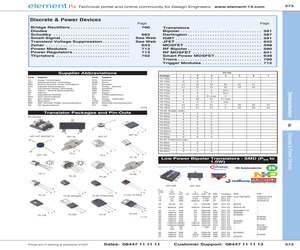
-- BD139-10 BD139-16 BD139G BD140-10 BD140-16 BD237G BD237 2N4923G BD179G BD435 BD437G BD439 BD441 2N5192 -- BFX34 BDX36 BUP41 2N3772 2N3716 TIP33C 2N3442 2N3772 2N3771 -- 2N3055 TIP3055 -- -- TIP2955 2N6254 MJ15015G 2N3055 2N3055H 2N3055H -- -- MJW21196G 2N3773G MJ15022G MJ15024G 2N3773 MJ15024 2N3773G -- -- -- MJ15003G 2N5038 MJ15003 -- -- TIP35C BD249C TIP35C BUW49 MJ802 2N6328 BUX98A BUV20 BUT30V 2SC2911 MJE350G MJE350 -- BD136 -- BD136-16 BD138 -- -- BD140G -- -- -- BD238 2N4920G BD180G BD436 BD438G -- -- 2N5195G BD438 -- -- BUP40 -- -- TIP34C -- -- -- MJ2955 -- -- PNP3055 MJ2955 -- -- MJ15016G -- -- -- TIP2955 MJW21195G -- 2N6609 MJ15023G MJ15025G -- -- -- MJ15023 MJ15025 MJE4353G MJ15004G -- MJ15004 MJ15004G 2N5883 TIP36C -- TIP36C -- -- 2N6331 -- -- -- 211280 Price Each Mftrs. List No. Mftr. BD135 BD136 BD136-16 BD138 BD139G BD139 BD139-10 BD139-16 BD140-10 BD140-16 BD140G BD179G BD180G BD237G BD237 BD238 BD249C BD250C BD434 BD435 ST ST ST ST ON ST ST ST ST ST ON ON ON ON ST
 144 Pages, 26045 KB, Original
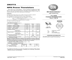
 VEBO 7 Vdc Collector Current - Continuous - Peak (Note 2) IC Base Current IB - Continuous - Peak (Note 2) Total Power Dissipation @ TA = 25C Derate above 25C Operating and Storage Junction Temperature Range Adc 16 30 Adc 4 15 PD TJ, Tstg TO-204 CASE 1-07 2N3773G MEX AYYWW 150 0.855 -65 to +200 A YY WW G = Assembly Location = Year = Work Week = Pb-Free Package W W/C ORDERING INFORMATION C See detailed ordering and shipping information in the package dimensions section on page 2 of this data sheet. Stresses exceeding Maximum Ratings may damage the device. Maximum Ratings are stress ratings only. Functional operation above the Recommended Operating Conditions is not implied. Extended exposure to stresses above the Recommended Operating Conditions may affect device reliability. 1. Indicates JEDEC Registered Data. 2. Pulse Test: Pulse Width = 5 ms, Duty Cycle v 10%. THERMAL CHARACTERISTICS Characteristic Thermal Resistance, Junction-to-Case Symbol Max Unit RqJC 1.17 C/W *For additional information on
 6 Pages, 128 KB, Original
 Semiconductor MOUSER STOCK NO. NPN (cont.) 863-TIP31BG 863-MJD44H11G 863-D44H11G 863-MJF44H11G 863-2N6488G 863-D44VH10G 863-2N5886G 863-2N5038G 863-MJ802G 863-TIP29CG 863-MJD31CG 863-TIP31CG 863-MJE243G 863-TIP41CG 863-TIP33CG 863-TIP35CG 863-2N3442G 863-2N3773G 863-MJF15030G 863-MMBT5551LT1G 863-MJE4343G 863-MJE344G 863-MMBTA42LT1G 863-BU406G 863-2N5655G 863-TIP47G 863-MJF47G 863-MJE340G 863-PZTA42T1G 863-TIP48G 863-MMBT6517LT1G 863-2N5657G 863-TIP50G 863-BUL45D2G 863-BUL146FG 863-MJE13007G 863-MJE13009G 863-BUX85G 863-MJE18004G 863-MJE18008G PNP 863-BCP69T1G 863-MMBT4126LT1G 863-MPS4126RLRAG 863-MJD210G 863-MJE210G 863-BC858BLT1G 863-BC858CLT1G 863-2N6111G 863-2N3906G 863-MMBT3906LT1G 863-MMBT3906WT1G 863-2N4403G 863-MMBT4403LT1G 863-MJE371G 863-TIP42G 863-MMBT5087LT1G 863-BC857BLT1G 863-BC807-16LT1G 863-BC807-25LT1G 863-BC807-40LT1G 863-BCX17LT1G 863-2N6109G 863-2SA1774G 863-MPSA55RLRAG 863-MMBTA55LT1G 863-MMBT2907ALT1G 863-MMBT2907AWT1G 863-MPS2907AG 863-PZT2907AT1G 863-MPS751RLRAG 863-TIP32
 379 Pages, 47721 KB, Original
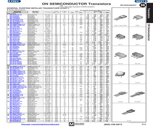
0.55 0.33 0.60 0.30 0.61 0.35 0.79 0.41 0.65 0.42 0.90 0.63 0.61 0.35 0.67 0.35 0.65 0.49 (4250) BIPOLAR POWER TRANSISTORS IN METAL TO-204AA PACKAGE NPN Mfg. Part No. 2N3771G 2N3055G 2N3055AG 2N3772G 2N5886G 2N5038G 2N6284G 2N5302G MJ802G MJ11016G 2N3442G 2N3773G MJ11022G VCEO(sus) Min. (V) 40 60 60 60 80 90 100 100 100 120 140 140 250 IC Max. (A) 30 15 15 20 25 20 20 30 30 30 10 16 15 60 80 100 100 120 120 140 250 200 250 250 15 25 12 20 15 30 20 15 16 16 16 Resistive Switching @ IC tf ts (A) (s) (s) ... ... ... 0.7 Typ. 0.3 Typ. 4 ... ... ... ... ... ... 1 0.8 10 1.5 0.5 12 2.5 Typ. 2.5 Typ. 10 2 1 30 ... ... ... ... ... ... ... ... ... 1.1 Typ. 1.5 Typ. 8 ... ... ... Price Each PD @ 25C (W) 150 115 115 150 200 140 160 200 200 200 117 150 175 Stock No. 26K5275 98H1011 42K3127 26K5276 26K5302 26K5286 26K5315 26K5293 26K4528 26K4505 26K5274 45J2472 42K1311 1-24 3.64 3.20 2.35 2.31 2.85 2.53 4.04 3.89 3.64 3.51 9.00 8.95 4.38 4.22 3.64 3.51 3.64 3.51 3.74 4.22 2.85 2.10 3.64 3.23 7.20 7.16 115 200
 375 Pages, 58008 KB, Original
 10 100 Package VCEO Max. (V) IC Max. (A) Min. MJE3055TG D44H8G 2N3055G TIP3055G BC846ALT1G BC846BLT1G BC846BWT1G 2N6292G MMBT8099LT1G MMBTA06LT1G TIP31BG MJE182G MJD44H11G D44H11G MJF44H11G 2N6488G D44VH10G 2N5038G TIP29CG MJD31CG TIP31CG MJE243G TIP41CG 2N3773G MJF15030G MMBT5551LT1G MMBTA42LT1G BU406G 2N5655G TIP47G MJF47G MMBTA42LT3G PZTA42T1G TIP48G MJE3439G 2N5657G TIP50G BUL45D2G MJE13007G BUX85G MJE18004G MJE18008G MJW18020G TO-220 TO-220 TO-3 TO-218 SOT-23 SOT-23 SC-70 TO-220 SOT-23 SOT-23 TO-220 Case 77 DPAK TO-220 TO-220FP TO-220 TO-220 TO-3 TO-220 DPAK TO-220 Case 77 TO-220 TO-3 TO-220FP SOT-23 SOT-23 TO-220 Case 77 TO-220 TO-220FP SOT-23 SOT-223 TO-220 TO-225 Case 77 TO-220 TO-220 TO-220 TO-220 TO-220 TO-220 TO-247 60 60 60 60 65 65 65 70 80 80 80 80 80 80 80 80 80 90 100 100 100 100 100 140 150 160 200 200 250 250 250 300 300 300 350 350 400 400 400 450 450 450 450 10 10 15 15 0.1 0.1 0.1 7 0.5 0.5 3 3 8 10 10 15 15 20 1 3 3 4 6 16 8 0.06 0.05 7 0.5 1 1 0.05 0.05 1 0.3 0.5 1 5 8 2 5
 1 Pages, 281 KB, Original
 VEBO 7 Vdc Collector Current - Continuous - Peak (Note 2) IC Base Current IB - Continuous - Peak (Note 2) Total Power Dissipation @ TA = 25C Derate above 25C Operating and Storage Junction Temperature Range Adc 16 30 Adc 4 15 PD TJ, Tstg TO-204 CASE 1-07 2N3773G MEX AYYWW 150 0.855 -65 to +200 A YY WW G = Assembly Location = Year = Work Week = Pb-Free Package W W/C ORDERING INFORMATION C See detailed ordering and shipping information in the package dimensions section on page 2 of this data sheet. Stresses exceeding Maximum Ratings may damage the device. Maximum Ratings are stress ratings only. Functional operation above the Recommended Operating Conditions is not implied. Extended exposure to stresses above the Recommended Operating Conditions may affect device reliability. 1. Indicates JEDEC Registered Data. 2. Pulse Test: Pulse Width = 5 ms, Duty Cycle v 10%. THERMAL CHARACTERISTICS Characteristic Thermal Resistance, Junction-to-Case Symbol Max Unit RqJC 1.17 C/W *For additional information on
 5 Pages, 116 KB, Original
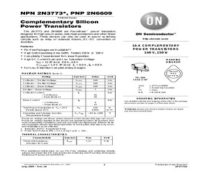
DOWN CHARACTERISTICS Second Breakdown Collector Current with Base Forward Biased t = 1 s (non-repetitive), VCE = 100 V, See Figure 12 3. Pulse Test: Pulse Width = 300 s, Duty Cycle 2%. 4. Indicates JEDEC Registered Data. ORDERING INFORMATION Device 2N3773 2N3773G 2N6609 Package Shipping TO-204 100 Unit / Tray TO-204 (Pb-Free) 100 Unit / Tray TO-204 100 Unit / Tray For information on tape and reel specifications, including part orientation and tape sizes, please refer to our Tape and Reel Packaging Specifications Brochure, BRD8011/D. http://onsemi.com 2 NPN 2N3773*, PNP 2N6609 NPN 300 200 PNP 300 200 150C 150C 100 100 -55 C 25C 70 hFE , DC CURRENT GAIN hFE , DC CURRENT GAIN 25C 50 VCE = 4 V 30 20 50 30 20 10 10 7.0 5.0 0.2 0.3 7.0 0.5 0.7 1.0 2.0 3.0 5.0 7.0 IC, COLLECTOR CURRENT (AMPS) 10 -55 C 70 VCE = 4 V 5.0 0.2 0.3 20 0.5 0.7 1.0 2.0 3.0 5.0 7.0 IC, COLLECTOR CURRENT (AMPS) 2.0 1.6 IC = 4 A 1.2 IC = 8 A IC = 16 A 0.8 0.4 TC = 25C 0 0.05 0.07 0.1 0.2 0.3 0.5 0.7 1.0 IB, BASE CURRENT (AMPS) 2.0
 6 Pages, 83 KB, Original
gh-Volume Device 2 = Moderate-Volume Device 3 = Low-Volume Device COMMERCIAL COMPONENTS EFFECTIVE DATE: OCTOBER 9, 2004 Type No. Per Unit Suggested Resale Price PC Qty Price Grp/Description Minimum Package Quantity 2N3773 A BIP T03 NPN 16A 140V 1 100 1.92 2N3773G A BIP T03 NPN 16A 140V 1 100 1.92 100 2N3819 A SS T092 JFET NCH 30V 2 1000 .227 1000 2N3903RLRM A SS T092 GP XSTR NPN 40V 2 2000 .0928 2000 2N3904 A SS T092 GP XSTR NPN 40V 2 5000 .032 5000 2N3904G A SS T092 GP XSTR NPN 40V 2 5000 .032 5000 2N3904RLRA A SS T092 GP XSTR NPN 40V 2 2000 .032 2000 2N3904RLRAG A SS T092 GP XSTR NPN 40V 2 2000 .032 2000 2N3904RLRM A SS T092 GP XSTR NPN 40V 2 2000 .032 2000 2N3904RLRMG A SS T092 GP XSTR NPN 40V 2 2000 .032 2000 2N3904RLRP A SS T092 GP XSTR NPN 40V 2 2000 .032 2000 2N3904RLRPG A SS T092 GP XSTR NPN 40V 2 2000 .032 2000 2N3904RL1 A SS T092 GP XSTR NPN 40V 2 2000 .032 2000 2N3904ZL1 A SS T092 GP XSTR NPN 40V 2 2000 .032 2000 2N3906 A SS T092 GP XSTR PNP 40V 2 5000 .032 5000 2N3906G A SS T092 GP XS
 296 Pages, 947 KB, Original
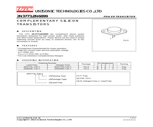
mplement Characterized for linear operation * High DC Current Gain and low saturation voltage hFE>15(8A, 4V) VCE(SAT)<1.4V(IC=8A, IB=0.8A) * For Low Distortion Complementary Designs ORDERING INFORMATION Ordering Number Lead Free Halogen Free 2N3773L-T30-Y 2N3773G-T30-Y 2N6099L-T30-Y 2N6099G-T30-Y www.unisonic.com.tw Copyright (c) 2012 Unisonic Technologies Co., LTD Package TO-3 TO-3 Pin Assignment 1 2 3 B E C B E C Packing Tray Tray 1 of 3 QW-R205-001,Ba 2N3773/2N6099 POWER TRANSISTOR ABSOLUTE MAXIMUM RATING (TA=25, unless otherwise specified ) PARAMETER SYMBOL RATINGS UNIT Collector-Base Voltage VCBO 160 V Collector-Emitter Voltage VCEO 140 V Emitter-Base Voltage VEBO 7 V Collector-Emitter Voltage VCEX 160 V TC=25 150 W Power Dissipation PC Dertate Above 25 0.855 W/ Continuous 16 A Collector Current IC Peak 30 A Continuous 4 A Base Current IB Peak 15 A Junction Temperature TJ 150 Storage Temperature TSTG -55 ~ +150 Note: 1. Absolute maximum ratings are those values beyond which the device could
 3 Pages, 147 KB, Original
DOWN CHARACTERISTICS Second Breakdown Collector Current with Base Forward Biased t = 1 s (non-repetitive), VCE = 100 V, See Figure 12 3. Pulse Test: Pulse Width = 300 s, Duty Cycle 2%. 4. Indicates JEDEC Registered Data. ORDERING INFORMATION Device 2N3773 2N3773G 2N6609 Package Shipping TO-204 100 Unit / Tray TO-204 (Pb-Free) 100 Unit / Tray TO-204 100 Unit / Tray For information on tape and reel specifications, including part orientation and tape sizes, please refer to our Tape and Reel Packaging Specifications Brochure, BRD8011/D. 2 NPN 2N3773*, PNP 2N6609 PACKAGE DIMENSIONS TO-204 (TO-3) CASE 1-07 ISSUE Z NOTES: 1. DIMENSIONING AND TOLERANCING PER ANSI Y14.5M, 1982. 2. CONTROLLING DIMENSION: INCH. 3. ALL RULES AND NOTES ASSOCIATED WITH REFERENCED TO-204AA OUTLINE SHALL APPLY. A N C -T- E D K 2 PL 0.13 (0.005) U T Q M M Y DIM A B C D E G H K L N Q U V M -Y- L V SEATING PLANE 2 H G B M T Y 1 -Q- 0.13 (0.005) M INCHES MIN MAX 1.550 REF --- 1.050 0.250 0.335 0.038 0.043 0.055 0.070 0.430 BSC 0.215
 3 Pages, 54 KB, Original
DOWN CHARACTERISTICS Second Breakdown Collector Current with Base Forward Biased t = 1 s (non-repetitive), VCE = 100 V, See Figure 12 3. Pulse Test: Pulse Width = 300 s, Duty Cycle 2%. 4. Indicates JEDEC Registered Data. ORDERING INFORMATION Device 2N3773 2N3773G 2N6609 Package Shipping TO-204 100 Unit / Tray TO-204 (Pb-Free) 100 Unit / Tray TO-204 100 Unit / Tray For information on tape and reel specifications, including part orientation and tape sizes, please refer to our Tape and Reel Packaging Specifications Brochure, BRD8011/D. http://onsemi.com 46 NPN 2N3773*, PNP 2N6609 NPN 300 200 PNP 300 200 150C 150C hFE , DC CURRENT GAIN hFE , DC CURRENT GAIN 25C 100 -55 C 25C 70 50 VCE = 4 V 30 20 100 50 30 20 10 10 7.0 5.0 0.2 0.3 7.0 0.5 0.7 1.0 2.0 3.0 5.0 7.0 IC, COLLECTOR CURRENT (AMPS) 10 -55 C 70 VCE = 4 V 5.0 0.2 0.3 20 0.5 0.7 1.0 2.0 3.0 5.0 7.0 IC, COLLECTOR CURRENT (AMPS) 2.0 1.6 IC = 4 A 1.2 IC = 8 A IC = 16 A 0.8 0.4 TC = 25C 0 0.05 0.07 0.1 0.2 0.3 0.5 0.7 1.0 IB, BASE CURRENT (AMPS) 2.
 4 Pages, 108 KB, Original


