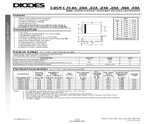
8.3ms Single Half Sine Wave Superimposed on Rated Load (Notes 2 & 3) Operating and Storage Temperature Range Electrical Characteristics Part Number Breakdown Voltage VBR @ IT (Note 5) See Notes 4, 6 3.0SMCJ5.0A 3.0SMCJ20A 3.0SMCJ22A 3.0SMCJ24A 3.0SMCJ28A 3.0SMCJ30A 3.0SMCJ58A VRWM (V) 5.0 20.0 22.0 24.0 28.0 30.0 58.0 Min (V) 6.40 22.20 24.40 26.70 31.10 33.30 64.40 1. 2. 3. 4. 5. 6. 7. Value 3000 Unit W IFSM 300 A Tj, TSTG -55 to +175 C @TA = 25C unless otherwise specified Reverse Standoff Voltage Notes: Symbol PPK Max (V) 7.07 24.5 27.0 29.5 34.4 36.8 71.2 Test Current Max. Reverse Leakage @ VRWM IT(mA) 10 1.0 1.0 1.0 1.0 1.0 1.0 IR (A) 1000 5.0 5.0 5.0 5.0 5.0 5.0 Max. Clamping Voltage @ Ipp VC (V) 9.2 32.4 35.5 38.9 45.4 48.4 93.6 Max. Peak Pulse Current Ipp Typical Total Capacitance (Note 7) Marking Code (A) 326.1 92.6 84.5 77.1 66.1 62.0 32.1 CT (pF) 8,000 3,300 3,000 3,000 1,800 1,700 1,500 HDE HEV HEX HEZ HFG HFK HGG Non-repetitive current pulse, per Fig. 4 and derated above TA = 25C per
 3 Pages, 73 KB, Original
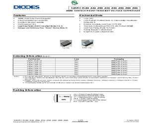
 (Matte Tin Finish) Polarity Indicator: Cathode Band Weight: 0.21 grams (Approximate) Bottom View Top View Ordering Information (Note 4) Notes: Part Number Case Packaging 3.0SMCJ5.0A-13 3.0SMCJ14A-13 3.0SMCJ20A-13 3.0SMCJ22A-13 3.0SMCJ24A-13 3.0SMCJ28A-13 3.0SMCJ30A-13 3.0SMCJ58A-13 SMC SMC SMC SMC SMC SMC SMC SMC 3000/Tape & Reel 3000/Tape & Reel 3000/Tape & Reel 3000/Tape & Reel 3000/Tape & Reel 3000/Tape & Reel 3000/Tape & Reel 3000/Tape & Reel 1. EU Directive 2002/95/EC (RoHS) & 2011/65/EU (RoHS 2) compliant. All applicable RoHS exemptions applied. 2. See http://www.diodes.com/quality/lead_free.html for more information about Diodes Incorporated's definitions of Halogen- and Antimony-free, "Green" and Lead-free. 3. Halogen- and Antimony-free "Green" products are defined as those which contain <900ppm bromine, <900ppm chlorine (<1500ppm total Br + Cl) and <1000ppm antimony compounds. 4. For packaging details, go to our website at http://www.diodes.com/products/packages.html. Marking Informatio
 5 Pages, 379 KB, Original
eristic Operating and Storage Temperature Range Electrical Characteristics @TA = 25C unless otherwise specified Part Number Reverse Standoff Voltage Breakdown Voltage VBR @ IT (Note 5) See Notes 4, 6 3.0SMCJ5.0A 3.0SMCJ20A 3.0SMCJ22A 3.0SMCJ24A 3.0SMCJ28A 3.0SMCJ30A 3.0SMCJ58A VRWM (V) 5.0 20.0 22.0 24.0 28.0 30.0 58.0 Min (V) 6.40 22.20 24.40 26.70 31.10 33.30 64.40 Notes: 1. 2. 3. 4. 5. 6. 7. Max (V) 7.07 24.5 27.0 29.5 34.4 36.8 71.2 Test Current Max. Reverse Leakage @ VRWM IT(mA) 10 1.0 1.0 1.0 1.0 1.0 1.0 IR (A) 1000 5.0 5.0 5.0 5.0 5.0 5.0 Max. Clamping Voltage @ Ipp VC (V) 9.2 32.4 35.5 38.9 45.4 48.4 93.6 Max. Peak Pulse Current Ipp Typical Total Capacitance (Note 7) Marking Code (A) 326.1 92.6 84.5 77.1 66.1 62.0 32.1 CT (pF) 8,000 3,300 3,000 3,000 1,800 1,700 1,500 HDE HEV HEX HEZ HFG HFK HGG Non-repetitive current pulse, per Fig. 4 and derated above TA = 25C per Fig. 1. Mounted on 8.00mm2 (0.013mm thick) land areas. Measured with 8.3ms single half sine-wave. Duty cycle = 4 pulses per
 3 Pages, 87 KB, Original
rating and Storage Temperature Range Electrical Characteristics @TA = 25C unless otherwise specified Part Number Reverse Standoff Voltage Breakdown Voltage VBR @ IT (Note 5) See Notes 4, 6 3.0SMCJ5.0A 3.0SMCJ14A 3.0SMCJ20A 3.0SMCJ22A 3.0SMCJ24A 3.0SMCJ28A 3.0SMCJ30A 3.0SMCJ58A VRWM (V) 5.0 14.0 20.0 22.0 24.0 28.0 30.0 58.0 Min (V) 6.40 15.60 22.20 24.40 26.70 31.10 33.30 64.40 Notes: Max (V) 7.07 17.2 24.5 27.0 29.5 34.4 36.8 71.2 Test Current Max. Reverse Leakage @ VRWM IT(mA) 10 1.0 1.0 1.0 1.0 1.0 1.0 1.0 IR (A) 1000 5.0 5.0 5.0 5.0 5.0 5.0 5.0 Max. Clamping Voltage @ Ipp VC (V) 9.2 23.2 32.4 35.5 38.9 45.4 48.4 93.6 Max. Peak Pulse Current Ipp Typical Total Capacitance (Note 7) Marking Code (A) 326.1 129.3 92.6 84.5 77.1 66.1 62.0 32.1 CT (pF) 8,000 3,500 3,300 3,000 3,000 1,800 1,700 1,500 HDE HEK HEV HEX HEZ HFG HFK HGG 1. Non-repetitive current pulse, per Fig. 4 and derated above TA = 25C per Fig. 1. 2. Mounted on 8.00mm2 (0.013mm thick) land areas. 3. Measured with 8.3ms single half sine
 4 Pages, 95 KB, Original
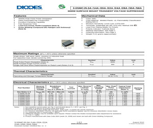
8 71.2 10 1 1 1 1 1 1 1000 5 5 5 5 5 5 9.2 32.4 35.5 38.9 45.4 48.4 93.6 326.1 92.6 84.5 77.1 66.1 62.0 32.1 Fig. 5 Fig. 5 Fig. 5 Fig. 5 Fig. 5 Fig. 5 Fig. 5 3000W Transient Voltage Suppressors / SMC 3.0SMCJ5.0A 3.0SMCJ20A 3.0SMCJ22A 3.0SMCJ24A 3.0SMCJ28A 3.0SMCJ30A 3.0SMCJ58A 3000 3000 3000 3000 3000 3000 3000 10x1000 10x1000 10x1000 10x1000 10x1000 10x1000 10x1000 5 20 22 24 28 30 58 () Reference product data sheet for specific conditions. All data is subject to change. Please check our data sheets at www.diodes.com for updates. Transient Voltage Suppressors (TVS) 14-7 Discrete Semiconductors Transient Voltage Suppressors (TVS) Transient Voltage Suppressor (TVS) Configurations Figure 1 Figure 2 Figure 3 Figure 4 Single Unidirectonal: PowerDI 123, SOD-523, SMA, SMB, SMC Figure 5 (R) Figure 7 DFN1006-2 Figure 6 Single Bi-Directional* SMA, SMB, SMC Figure 8 DLPD3V3LC * 'C' suffix in part number denotes bi-directional device. Transient Voltage Suppressors (TVS) 14-8 All data is subject to change. P
 173 Pages, 2488 KB, Original
rating and Storage Temperature Range Electrical Characteristics @TA = 25C unless otherwise specified Part Number Reverse Standoff Voltage Breakdown Voltage VBR @ IT (Note 5) See Notes 4, 6 3.0SMCJ5.0A 3.0SMCJ14A 3.0SMCJ20A 3.0SMCJ22A 3.0SMCJ24A 3.0SMCJ28A 3.0SMCJ30A 3.0SMCJ58A VRWM (V) 5.0 14.0 20.0 22.0 24.0 28.0 30.0 58.0 Min (V) 6.40 15.60 22.20 24.40 26.70 31.10 33.30 64.40 Notes: Max (V) 7.07 17.2 24.5 27.0 29.5 34.4 36.8 71.2 Test Current Max. Reverse Leakage @ VRWM IT(mA) 10 1.0 1.0 1.0 1.0 1.0 1.0 1.0 IR (A) 1000 5.0 5.0 5.0 5.0 5.0 5.0 5.0 Max. Clamping Voltage @ Ipp VC (V) 9.2 23.2 32.4 35.5 38.9 45.4 48.4 93.6 Max. Peak Pulse Current Ipp Typical Total Capacitance (Note 7) Marking Code (A) 326.1 129.3 92.6 84.5 77.1 66.1 62.0 32.1 CT (pF) 8,000 3,500 3,300 3,000 3,000 1,800 1,700 1,500 HDE HEK HEV HEX HEZ HFG HFK HGG 1. Non-repetitive current pulse, per Fig. 4 and derated above TA = 25C per Fig. 1. 2. Mounted on 8.00mm2 (0.013mm thick) land areas. 3. Measured with 8.3ms single half sine
 4 Pages, 90 KB, Original
 (Matte Tin Finish) Polarity Indicator: Cathode Band Weight: 0.21 grams (Approximate) Bottom View Top View Ordering Information (Note 4) Notes: Part Number Case Packaging 3.0SMCJ5.0A-13 3.0SMCJ14A-13 3.0SMCJ20A-13 3.0SMCJ22A-13 3.0SMCJ24A-13 3.0SMCJ28A-13 3.0SMCJ30A-13 3.0SMCJ58A-13 SMC SMC SMC SMC SMC SMC SMC SMC 3000/Tape & Reel 3000/Tape & Reel 3000/Tape & Reel 3000/Tape & Reel 3000/Tape & Reel 3000/Tape & Reel 3000/Tape & Reel 3000/Tape & Reel 1. EU Directive 2002/95/EC (RoHS) & 2011/65/EU (RoHS 2) compliant. All applicable RoHS exemptions applied. 2. See http://www.diodes.com/quality/lead_free.html for more information about Diodes Incorporated's definitions of Halogen- and Antimony-free, "Green" and Lead-free. 3. Halogen- and Antimony-free "Green" products are defined as those which contain <900ppm bromine, <900ppm chlorine (<1500ppm total Br + Cl) and <1000ppm antimony compounds. 4. For packaging details, go to our website at http://www.diodes.com/products/packages.html. Marking Informatio
 4 Pages, 385 KB, Original
 Range Electrical Characteristics @TA = 25C unless otherwise specified Part Number Reverse Standoff Voltage Breakdown Voltage VBR @ IT (Note 5) Test Current Max. Reverse Leakage @ VRWM See Notes 4, 6 3.0SMCJ5.0A 3.0SMCJ20A 3.0SMCJ22A 3.0SMCJ24A 3.0SMCJ28A 3.0SMCJ30A 3.0SMCJ58A VRWM (V) 5.0 20.0 22.0 24.0 28.0 30.0 58.0 Min (V) 6.40 22.20 24.40 26.70 31.10 33.30 64.40 IT(mA) 10 1.0 1.0 1.0 1.0 1.0 1.0 IR (A) 1000 5.0 5.0 5.0 5.0 5.0 5.0 Notes: 1. 2. 3. 4. 5. 6. 7. 8. Max (V) 7.07 24.5 27.0 29.5 34.4 36.8 71.2 Max. Clamping Voltage @ Ipp VC (V) 9.2 32.4 35.5 38.9 45.4 48.4 93.6 Max. Peak Pulse Current Ipp Typical Total Capacitance (Note 7) Marking Code (A) 326.1 92.6 84.5 77.1 66.1 62.0 32.1 CT (pF) 8,000 3,300 3,000 3,000 1,800 1,700 1,500 HDE HEV HEX HEZ HFG HFK HGG Non-repetitive current pulse, per Fig. 4 and derated above TA = 25C per Fig. 1. Mounted on 8.00mm2 (0.013mm thick) land areas. Measured with 8.3ms single half sine-wave. Duty cycle = 4 pulses per minute maximum. EU Directive 2002/95/E
 4 Pages, 108 KB, Original
e Breakdown Voltage VBR @ IT (Note 5) Test Current Max. Reverse Leakage @ VRWM Max. Clamping Voltage @ Ipp Max. Peak Pulse Current Ipp See Notes 4, 6 VRWM (V) Min (V) Max (V) IT(mA) IR (A) VC (V) (A) 3.0SMCJ5.0A 3.0SMCJ20A 3.0SMCJ22A 3.0SMCJ24A 3.0SMCJ28A 3.0SMCJ30A 3.0SMCJ58A 5.0 20.0 22.0 24.0 28.0 30.0 58.0 6.40 22.20 24.40 26.70 31.10 33.30 64.40 7.07 24.5 27.0 29.5 34.4 36.8 71.2 10 1.0 1.0 1.0 1.0 1.0 1.0 1000 5.0 5.0 5.0 5.0 5.0 5.0 9.2 32.4 35.5 38.9 45.4 48.4 93.6 326.1 92.6 84.5 77.1 66.1 62.0 32.1 Notes: 1. 2. 3. 4. 5. 6. Typical Total Capacitance CT @ f = 1MHz (pF) 8,000 3,300 3,000 3,000 1,800 1,700 1,500 Marking Code HDE HEV HEX HEZ HFG HFK HGG Non-repetitive current pulse, per Fig. 4 and derated above TA = 25C per Fig. 1. Mounted on 8.00mm2 (0.013mm thick) land areas. Measured with 8.3ms single half sine-wave. Duty cycle = 4 pulses per minute maximum. RoHS revision 13.2.2003. Glass and high temperature solder exemptions applied, see EU Directive Annex Notes 5 and 7. VBR measured wi
 3 Pages, 74 KB, Original
2 2W02G N/A 2W02G 2W02G N/A 2W04 2W04G N/A 2W04G 2W04G N/A 2W06 2W06G N/A 2W06G 2W06G N/A 2W08 2W08G N/A 2W08G 2W08G N/A 2W10 2W10G N/A 2W10G 2W10G N/A 3.0SMCJ20A 3.0SMCJ20A N/A 3.0SMCJ22A 3.0SMCJ22A N/A 3.0SMCJ24A 3.0SMCJ24A N/A 3.0SMCJ28A 3.0SMCJ28A N/A 3.0SMCJ30A 3.0SMCJ30A N/A 3.0SMCJ5.0A 3.0SMCJ5.0A N/A 3.0SMCJ58A 3.0SMCJ58A N/A 30BF10 ES3B N/A 30BF20 ES3D N/A 30BQ015 N/A PDS340 30BQ015 N/A B320 30BQ020 B320 PDS340 30BQ030 B330 PDS340 30BQ040 N/A B340 30BQ040 N/A PDS340 30BQ050 B350 N/A 30BQ060 B360 30BQ070 B370 30BQ080 B380 30BQ090 B390 30BQ100 B3100 30CPQ045 30CPQ060 30CTQ035 30CTQ040 30CTQ045S 30CTQ060PbF 30CTQ060S 30L30CT N/A 30S1 1N5401 30S10 1N5408 30S2 1N5402 30S3 1N5404 30S4 1N5404 30S5 1N5406 30S6 1N5406 30S8 1N5407 31DQ0100 31DQ015 N/A 31DQ020 SB320 31DQ030 SB330 31DQ04 SB340 31DQ040 SB340 31DQ05 SB350 31DQ050 SB350 31DQ06 SB360 31DQ10 SB3100 31DQ100 SB3100 32CTQ030 32CTQ030S 3E05 1N5400 3E1 1N5401 3E10 1N5408 3E2 1N5402 3E4 1N5404 3E6 1N5406 3E8 1N5407 3N246 N/A 3N247
 257 Pages, 363 KB, Original
rating and Storage Temperature Range Electrical Characteristics @TA = 25C unless otherwise specified Part Number Reverse Standoff Voltage Breakdown Voltage VBR @ IT (Note 5) See Notes 4, 6 3.0SMCJ5.0A 3.0SMCJ14A 3.0SMCJ20A 3.0SMCJ22A 3.0SMCJ24A 3.0SMCJ28A 3.0SMCJ30A 3.0SMCJ58A VRWM (V) 5.0 14.0 20.0 22.0 24.0 28.0 30.0 58.0 Min (V) 6.40 15.60 22.20 24.40 26.70 31.10 33.30 64.40 Notes: 1. 2. 3. 4. 5. 6. 7. 8. Max (V) 7.07 17.2 24.5 27.0 29.5 34.4 36.8 71.2 Test Current Max. Reverse Leakage @ VRWM IT(mA) 10 1.0 1.0 1.0 1.0 1.0 1.0 1.0 IR (A) 1000 5.0 5.0 5.0 5.0 5.0 5.0 5.0 Max. Clamping Voltage @ Ipp VC (V) 9.2 23.2 32.4 35.5 38.9 45.4 48.4 93.6 Max. Peak Pulse Current Ipp Typical Total Capacitance (Note 7) Marking Code (A) 326.1 129.3 92.6 84.5 77.1 66.1 62.0 32.1 CT (pF) 8,000 3,500 3,300 3,000 3,000 1,800 1,700 1,500 HDE HEK HEV HEX HEZ HFG HFK HGG Non-repetitive current pulse, per Fig. 4 and derated above TA = 25C per Fig. 1. Mounted on 8.00mm2 (0.013mm thick) land areas. Measured with 8.3ms s
 4 Pages, 109 KB, Original
Z6 --- 24.5 --- 29.5 1 5.0 50.0 110.0 3.0SMCJ26 3.0SMCJ26C HFD IFD 26.0 28.9 35.3 1 5 46.6 64.4 3.0SMCJ26A 3.0SMCJ26CA HFE IFE 26.0 28.9 31.9 1 5 42.1 71.3 Type Number (UNI) Type Number (BI) 3.0SMCJ28 3.0SMCJ28C 3.0SMCJ28A 3.0SMCJ28CA 3.0SMCJ30 3.0SMCJ30C 3.0SMCJ30A 3.0SMCJ30CA 3.0SMCJ33 3.0SMCJ33C 3.0SMCJ33A 3.0SMCJ33CA 3.0SMCJ33A6 3.0SMCJ36 3.0SMCJ36C 3.0SMCJ36A 3.0SMCJ36CA 3.0SMCJ36A6 Device Marking code (UNI) Reverse Standoff Voltage Breakdown Voltage BV Volts @It Max. Reverse Leakage @VR Max. Clamping Voltage @Ipp Max. Peak Pulse Current (BI) VR (V) Min (V) Max (V) It (mA) IR (uA) Vc (V) Ipp (A) HFF IFF 28.0 31.1 38.0 1 5 50.0 60.0 HFG IFG 28.0 31.1 34.4 1 5 45.4 66.1 HFH IFH 30.0 33.3 40.7 1 5 53.5 56.1 HFK IFK 30.0 33.3 36.8 1 5 48.4 62.0 HFL IFL 33.0 36.7 44.8 1 5 59.0 50.8 HFM IFM 33.0 36.7 40.6 1 5 53.3 56.3 HFM6 --- 33.0 36.7 40.6 1 5 54.3 70.0 HFN IFN 36.0 40.0 48.9 1 5 64.3 46.7 HFP IFP 36.0 40.0 44.2 1 5 58.1 51.6 HFP6 --- 36.0 40.0 44.2 1 5 59.1 70.0 3.0SMCJ40 3.0SMCJ40C HFQ IFQ 40
 5 Pages, 131 KB, Original
1.0 24 5 43.0 69.8 3.0SMCJ24A 26.7 30.7 1.0 24 5 38.9 77.2 3.0SMCJ26 28.9 36.6 1.0 26 5 46.6 64.4 3.0SMCJ26A 28.9 33.2 1.0 26 5 42.1 71.2 3.0SMCJ28 31.1 39.4 1.0 28 5 50.0 60.0 3.0SMCJ28A 31.1 35.8 1.0 28 5 45.4 66.0 3.0SMCJ30 33.3 42.2 1.0 30 5 53.5 56.0 3.0SMCJ30A 33.3 38.3 1.0 30 5 48.4 62.0 3.0SMCJ33 36.7 46.5 1.0 33 5 59.0 50.4 3.0SMCJ33A 36.7 42.2 1.0 33 5 53.3 56.2 3.0SMCJ36 40.0 50.7 1.0 36 5 64.3 46.6 3.0SMCJ36A 40.0 46.0 1.0 36 5 58.1 51.6 3.0SMCJ40 44.4 56.3 1.0 40 5 71.4 42.0 3.0SMCJ40A 44.4 51.1 1.0 40 5 64.5 46.4 3.0SMCJ43 47.8 60.5 1.0 43 5 76.7 39.2 3.0SMCJ43A 47.8 54.9 1.0 43 5 69.4 43.2 3.0SMCJ45 50.0 63.3 1.0 45 5 80.3 37.4 3.0SMCJ45A 50.0 57.5 1.0 45 5 72.7 41.2 3.0SMCJ48 53.3 67.5 1.0 48 5 85.5 35.0 3.0SMCJ48A 53.3 61.3 1.0 48 5 77.4 38.8 3.0SMCJ51 56.7 71.8 1.0 51 5 91.1 37.0 3.0SMCJ51A 56.7 65.2 1.0 51 5 82.4 36.4 3.0SMCJ54 60.0 76.0 1.0 54 5 96.3 31.2 3.0SMCJ54A 60.0 69.0 1.0 54 5 87.1 34.4 Breakdown Voltage @ IT (1) Type VBR (V) Page 2 of 4 Working Peak Reverse Voltage Ma
 4 Pages, 65 KB, Original
J12 3.0SMCJ12A 3.0SMCJ13 3.0SMCJ13A 3.0SMCJ14 3.0SMCJ14A 3.0SMCJ15 3.0SMCJ15A 3.0SMCJ16 3.0SMCJ16A 3.0SMCJ17 3.0SMCJ17A 3.0SMCJ18 3.0SMCJ18A 3.0SMCJ20 3.0SMCJ20A 3.0SMCJ22 3.0SMCJ22A 3.0SMCJ24 3.0SMCJ24A 3.0SMCJ26 3.0SMCJ26A 3.0SMCJ28 3.0SMCJ28A 3.0SMCJ30 3.0SMCJ30A 3.0SMCJ33 3.0SMCJ33A 3.0SMCJ36 3.0SMCJ36A 3.0SMCJ40 3.0SMCJ40A 3.0SMCJ43 3.0SMCJ43A 3.0SMCJ45 3.0SMCJ45A 3.0SMCJ48 3.0SMCJ48A 3.0SMCJ51 3.0SMCJ51A 3.0SMCJ54 3.0SMCJ54A 3.0SMCJ58 3.0SMCJ58A T 3013 3513 3014 3514 3015 3515 3016 3516 3018 3518 3019 3519 3020 3520 3021 3521 3023 3523 3026 3526 3028 3528 3030 3530 3033 3533 3035 3535 3039 3539 3042 3542 3047 3547 3050 3550 3053 3553 3056 3556 3060 3560 3063 3563 3068 3568 Working Peak Reverse Voltage Maximum Clamping Voltage @ IPPM Maximum Peak Pulse Surge Current Rev. 05 : June 10, 2006 Certificate TH97/10561QM Certificate TW00/17276EM ELECTRICAL CHARACTERISTICS Rating at 25 C ambient temperature unless otherwise specified VRWM VC IPPM Min. Max. IT (mA) Maximum Reverse Leakage @ VWM IR (V
 4 Pages, 50 KB, Original
J12 3.0SMCJ12A 3.0SMCJ13 3.0SMCJ13A 3.0SMCJ14 3.0SMCJ14A 3.0SMCJ15 3.0SMCJ15A 3.0SMCJ16 3.0SMCJ16A 3.0SMCJ17 3.0SMCJ17A 3.0SMCJ18 3.0SMCJ18A 3.0SMCJ20 3.0SMCJ20A 3.0SMCJ22 3.0SMCJ22A 3.0SMCJ24 3.0SMCJ24A 3.0SMCJ26 3.0SMCJ26A 3.0SMCJ28 3.0SMCJ28A 3.0SMCJ30 3.0SMCJ30A 3.0SMCJ33 3.0SMCJ33A 3.0SMCJ36 3.0SMCJ36A 3.0SMCJ40 3.0SMCJ40A 3.0SMCJ43 3.0SMCJ43A 3.0SMCJ45 3.0SMCJ45A 3.0SMCJ48 3.0SMCJ48A 3.0SMCJ51 3.0SMCJ51A 3.0SMCJ54 3.0SMCJ54A 3.0SMCJ58 3.0SMCJ58A 3.0SMCJ60 3.0SMCJ60A 3.0SMCJ64 3.0SMCJ64A 3.0SMCJ70 3.0SMCJ70A 3.0SMCJ75 3.0SMCJ75A 3.0SMCJ78 3.0SMCJ78A 3.0SMCJ85 3.0SMCJ85A 3.0SMCJ90 3.0SMCJ90A 3.0SMCJ100 3.0SMCJ100A 3.0SMCJ110 3.0SMCJ110A 3.0SMCJ120 3.0SMCJ120A 3.0SMCJ130 3.0SMCJ130A 3.0SMCJ150 3.0SMCJ150A 3.0SMCJ160 3.0SMCJ160A 3.0SMCJ170 3.0SMCJ170A 3.0SMCJ SERIES REVERSE STAND-OFF VOLTAGE VRWM (V) BREAKDOWN VOLTAGE VBR (V) MIN. @IT BREAKDOWN VOLTAGE VBR (V) MAX. @IT 5.00 5.00 6.00 6.00 6.50 6.50 7.00 7.00 7.50 7.50 8.00 8.00 8.50 8.50 9.00 9.00 10.00 10.00 11.00 11.00 12.00 12.00 13.00 13.00
 4 Pages, 51 KB, Original


