ins Package Qty Drawing Eco Plan Lead/Ball Finish (2) MSL Peak Temp Samples (3) (Requires Login) ADC108S052CIMT ACTIVE TSSOP PW 16 92 TBD CU SNPB Level-1-260C-UNLIM ADC108S052CIMT/NOPB ACTIVE TSSOP PW 16 92 Green (RoHS & no Sb/Br) CU SN Level-1-260C-UNLIM ADC108S052CIMTX ACTIVE TSSOP PW 16 2500 TBD CU SNPB Level-1-260C-UNLIM ADC108S052CIMTX/NOPB ACTIVE TSSOP PW 16 2500 Green (RoHS & no Sb/Br) CU SN Level-1-260C-UNLIM (1) The marketing status values are defined as follows: ACTIVE: Product device recommended for new designs. LIFEBUY: TI has announced that the device will be discontinued, and a lifetime-buy period is in effect. NRND: Not recommended for new designs. Device is in production to support existing customers, but TI does not recommend using this part in a new design. PREVIEW: Device has been announced but is not in production. Samples may or may not be available. OBSOLETE: TI has discontinued the production of the device. (2) Eco Plan - The planned eco-friendly classification
 23 Pages, 1097 KB, Original
ish (2) MSL Peak Temp Op Temp (C) Top-Side Markings (3) (4) ADC108S052CIMT ACTIVE TSSOP PW 16 92 TBD Call TI Call TI -40 to 105 108S052 CIMT ADC108S052CIMT/NOPB ACTIVE TSSOP PW 16 92 Green (RoHS & no Sb/Br) CU SN Level-1-260C-UNLIM -40 to 105 108S052 CIMT ADC108S052CIMTX ACTIVE TSSOP PW 16 2500 TBD Call TI Call TI -40 to 105 108S052 CIMT ADC108S052CIMTX/NOPB ACTIVE TSSOP PW 16 2500 Green (RoHS & no Sb/Br) CU SN Level-1-260C-UNLIM -40 to 105 108S052 CIMT (1) The marketing status values are defined as follows: ACTIVE: Product device recommended for new designs. LIFEBUY: TI has announced that the device will be discontinued, and a lifetime-buy period is in effect. NRND: Not recommended for new designs. Device is in production to support existing customers, but TI does not recommend using this part in a new design. PREVIEW: Device has been announced but is not in production. Samples may or may not be available. OBSOLETE: TI has discontinued the production of the device. (2) Eco Plan - Th
 27 Pages, 1147 KB, Original
ce Status (1) Package Type Package Pins Package Drawing Qty Eco Plan (2) Lead finish/ Ball material MSL Peak Temp Op Temp (C) Device Marking (3) (4/5) (6) ADC108S052CIMT/NOPB ACTIVE TSSOP PW 16 92 RoHS & Green SN Level-1-260C-UNLIM -40 to 105 108S052 CIMT ADC108S052CIMTX/NOPB ACTIVE TSSOP PW 16 2500 RoHS & Green SN Level-1-260C-UNLIM -40 to 105 108S052 CIMT (1) The marketing status values are defined as follows: ACTIVE: Product device recommended for new designs. LIFEBUY: TI has announced that the device will be discontinued, and a lifetime-buy period is in effect. NRND: Not recommended for new designs. Device is in production to support existing customers, but TI does not recommend using this part in a new design. PREVIEW: Device has been announced but is not in production. Samples may or may not be available. OBSOLETE: TI has discontinued the production of the device. (2) RoHS: TI defines "RoHS" to mean semiconductor products that are compliant with the current EU RoHS requirements for all 10 R
 29 Pages, 1274 KB, Original
ce Status (1) Package Type Package Pins Package Drawing Qty Eco Plan Lead/Ball Finish (2) MSL Peak Temp Op Temp (C) Device Marking (3) (4/5) ADC108S052CIMT/NOPB ACTIVE TSSOP PW 16 92 Green (RoHS & no Sb/Br) CU SN Level-1-260C-UNLIM -40 to 105 108S052 CIMT ADC108S052CIMTX/NOPB ACTIVE TSSOP PW 16 2500 Green (RoHS & no Sb/Br) CU SN Level-1-260C-UNLIM -40 to 105 108S052 CIMT (1) The marketing status values are defined as follows: ACTIVE: Product device recommended for new designs. LIFEBUY: TI has announced that the device will be discontinued, and a lifetime-buy period is in effect. NRND: Not recommended for new designs. Device is in production to support existing customers, but TI does not recommend using this part in a new design. PREVIEW: Device has been announced but is not in production. Samples may or may not be available. OBSOLETE: TI has discontinued the production of the device. (2) Eco Plan - The planned eco-friendly classification: Pb-Free (RoHS), Pb-Free (RoHS Exempt), or Green (RoHS & no
 26 Pages, 1145 KB, Original
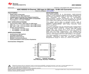
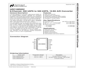
tomotive Navigation Portable Systems Medical Instruments Mobile Communications Instrumentation and Control Systems Connection Diagram 20164405 Ordering Information Order Code Temperature Range Description ADC108S052CIMT -40C to +105C 16-Lead TSSOP Package ADC108S052CIMTX -40C to +105C 16-Lead TSSOP Package, Tape & Reel ADC108S052EVAL Evaluation Board TRI-STATE (R) is a trademark of National Semiconductor Corporation. MICROWIRETM is a trademark of National Semiconductor Corporation. QSPITM and SPITM are trademarks of Motorola, Inc. (c) 2006 National Semiconductor Corporation DS201644 www.national.com ADC108S052 8-Channel, 200 kSPS to 500 kSPS, 10-Bit A/D Converter October 2006 ADC108S052 Block Diagram 20164407 Pin Descriptions and Equivalent Circuits Pin No. Symbol Equivalent Circuit Description ANALOG I/O 4 - 11 IN0 to IN7 Analog inputs. These signals can range from 0V to VREF. 16 SCLK Digital clock input. The guaranteed performance range of frequencies for this input is 3.2 MHz to 8 MHz. This cl
 17 Pages, 809 KB, Original
tomotive Navigation Portable Systems Medical Instruments Mobile Communications Instrumentation and Control Systems Connection Diagram 20164405 Ordering Information Temperature Range Description ADC108S052CIMT Order Code -40C to +105C 16-Lead TSSOP Package ADC108S052CIMTX -40C to +105C 16-Lead TSSOP Package, Tape & Reel ADC108S052EVAL Evaluation Board SPITM is a trademark of Motorola, Inc. (c) 2009 National Semiconductor Corporation 201644 www.national.com ADC108S052 8-Channel, 200 ksps to 500 ksps, 10-Bit A/D Converter June 2, 2009 ADC108S052 Block Diagram 20164407 Pin Descriptions and Equivalent Circuits Pin No. Symbol Equivalent Circuit Description ANALOG I/O 4 - 11 IN0 to IN7 Analog inputs. These signals can range from 0V to VREF. DIGITAL I/O 16 SCLK Digital clock input. The guaranteed performance range of frequencies for this input is 3.2 MHz to 8 MHz. This clock directly controls the conversion and readout processes. 15 DOUT Digital data output. The output samples are clocked out of this pin
 18 Pages, 354 KB, Original
tomotive Navigation Portable Systems Medical Instruments Mobile Communications Instrumentation and Control Systems Connection Diagram 20164405 Ordering Information Temperature Range Description ADC108S052CIMT Order Code -40C to +105C 16-Lead TSSOP Package ADC108S052CIMTX -40C to +105C 16-Lead TSSOP Package, Tape & Reel ADC108S052EVAL Evaluation Board SPITM is a trademark of Motorola, Inc. (c) 2011 National Semiconductor Corporation 201644 www.national.com ADC108S052 8-Channel, 200 ksps to 500 ksps, 10-Bit A/D Converter January 28, 2011 ADC108S052 Block Diagram 20164407 Pin Descriptions and Equivalent Circuits Pin No. Symbol Equivalent Circuit Description ANALOG I/O 4 - 11 IN0 to IN7 Analog inputs. These signals can range from 0V to VREF. DIGITAL I/O 16 SCLK Digital clock input. The guaranteed performance range of frequencies for this input is 3.2 MHz to 8 MHz. This clock directly controls the conversion and readout processes. 15 DOUT Digital data output. The output samples are clocked out of this
 18 Pages, 351 KB, Original
tomotive Navigation Portable Systems Medical Instruments Mobile Communications Instrumentation and Control Systems Connection Diagram 20164405 Ordering Information Order Code Temperature Range Description ADC108S052CIMT -40C to +105C 16-Lead TSSOP Package ADC108S052CIMTX -40C to +105C 16-Lead TSSOP Package, Tape & Reel ADC108S052EVAL Evaluation Board TRI-STATE (R) is a trademark of National Semiconductor Corporation. MICROWIRETM is a trademark of National Semiconductor Corporation. QSPITM and SPITM are trademarks of Motorola, Inc. (c) 2005 National Semiconductor Corporation DS201644 www.national.com ADC108S052 8-Channel, 200 kSPS to 500 kSPS, 10-Bit A/D Converter September 2005 ADC108S052 Block Diagram 20164407 Pin Descriptions and Equivalent Circuits Pin No. Symbol Equivalent Circuit Description ANALOG I/O 4 - 11 IN0 to IN7 Analog inputs. These signals can range from 0V to VREF. 16 SCLK Digital clock input. The guaranteed performance range of frequencies for this input is 8 MHz to 16 MHz. This c
 17 Pages, 809 KB, Original
tomotive Navigation Portable Systems Medical Instruments Mobile Communications Instrumentation and Control Systems Connection Diagram 20164405 Ordering Information Temperature Range Description ADC108S052CIMT Order Code -40C to +105C 16-Lead TSSOP Package ADC108S052CIMTX -40C to +105C 16-Lead TSSOP Package, Tape & Reel ADC108S052EVAL Evaluation Board SPITM is a trademark of Motorola, Inc. (c) 2008 National Semiconductor Corporation 201644 www.national.com ADC108S052 8-Channel, 200 ksps to 500 ksps, 10-Bit A/D Converter August 4, 2008 ADC108S052 Block Diagram 20164407 Pin Descriptions and Equivalent Circuits Pin No. Symbol Equivalent Circuit Description ANALOG I/O 4 - 11 IN0 to IN7 Analog inputs. These signals can range from 0V to VREF. DIGITAL I/O 16 SCLK Digital clock input. The guaranteed performance range of frequencies for this input is 3.2 MHz to 8 MHz. This clock directly controls the conversion and readout processes. 15 DOUT Digital data output. The output samples are clocked out of this p
 18 Pages, 336 KB, Original
tomotive Navigation Portable Systems Medical Instruments Mobile Communications Instrumentation and Control Systems Connection Diagram 20164405 Ordering Information Temperature Range Description ADC108S052CIMT Order Code -40C to +105C 16-Lead TSSOP Package ADC108S052CIMTX -40C to +105C 16-Lead TSSOP Package, Tape & Reel ADC108S052EVAL Evaluation Board SPITM is a trademark of Motorola, Inc. (c) 2011 National Semiconductor Corporation 201644 www.national.com ADC108S052 8-Channel, 200 ksps to 500 ksps, 10-Bit A/D Converter January 28, 2011 ADC108S052 Block Diagram 20164407 Pin Descriptions and Equivalent Circuits Pin No. Symbol Equivalent Circuit Description ANALOG I/O 4 - 11 IN0 to IN7 Analog inputs. These signals can range from 0V to VREF. DIGITAL I/O 16 SCLK Digital clock input. The guaranteed performance range of frequencies for this input is 3.2 MHz to 8 MHz. This clock directly controls the conversion and readout processes. 15 DOUT Digital data output. The output samples are clocked out of this
 20 Pages, 390 KB, Original
tomotive Navigation Portable Systems Medical Instruments Mobile Communications Instrumentation and Control Systems Connection Diagram 20164405 Ordering Information Temperature Range Description ADC108S052CIMT Order Code -40C to +105C 16-Lead TSSOP Package ADC108S052CIMTX -40C to +105C 16-Lead TSSOP Package, Tape & Reel ADC108S052EVAL Evaluation Board SPITM is a trademark of Motorola, Inc. (c) 2010 National Semiconductor Corporation 201644 www.national.com ADC108S052 8-Channel, 200 ksps to 500 ksps, 10-Bit A/D Converter February 8, 2010 ADC108S052 Block Diagram 20164407 Pin Descriptions and Equivalent Circuits Pin No. Symbol Equivalent Circuit Description ANALOG I/O 4 - 11 IN0 to IN7 Analog inputs. These signals can range from 0V to VREF. DIGITAL I/O 16 SCLK Digital clock input. The guaranteed performance range of frequencies for this input is 3.2 MHz to 8 MHz. This clock directly controls the conversion and readout processes. 15 DOUT Digital data output. The output samples are clocked out of this
 18 Pages, 354 KB, Original
ption vs. ThroughputADC108S052 (PC) (tN) (PN) 15 www.national.com/jpn/ ADC108S052 ADC108S052 2.0 ADC108S052 2.0 ( ) ( ) 1 2.3 S/E ( ) (I/O) ADC108S052 ADC108S052 90 / www.national.com/jpn/ 16 inches (millimeters) 16-Lead TSSOP Order Number ADC108S052CIMT, ADC108S052CIMTX NS Package Number MTC16 ( ) (CEO) (GENERAL COUNSEL) (a) (b) National Semiconductor Copyright (c) 2007 National Semiconductor Corporation www.national.com 135-0042 2-17-16 / TEL.(03)5639-7300 www.national.com/jpn/ ADC108S052 8 200kSPS 500kSPS10 A/D
 17 Pages, 650 KB, Original
ower Consumption vs. ThroughputADC108S052 (PC) (tN) (PN) 15 www.national.com/jpn/ ADC108S052 2.0 ADC108S052 2.0 ( ) ( ) 1 2.3 S/E ( ) (I/O) ADC108S052 ADC108S052 90 / www.national.com/jpn/ 16 inches (millimeters) 16-Lead TSSOP Order Number ADC108S052CIMT, ADC108S052CIMTX NS Package Number MTC16 (CEO) (GENERAL COUNSEL) a (b) National Semiconductor Copyright (c) 2007 National Semiconductor Corporation www.national.com 135-0042 2-17-16 / TEL.(03)5639-7300 www.national.com/jpn/ ADC108S052 8 200kSPS 500kSPS10 A/D
 17 Pages, 338 KB, Original


