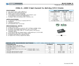
BAS316WS Taiwan Semiconductor 250mA, 100V High-Speed Switching SMD Diode FEATURES KEY PARAMETERS Low power loss, high efficiency Ideal for automated placement High surge current capability Compliance to RoHS directive 2011/65/EU and in accordance to WEEE 2002/96/EC Halogen-free according to IEC 61249-2-21 PARAMETER VALUE UNIT IF(AV) 250 mA VRRM 100 V VF at IF=150mA 1.25 V TJ Max. 150 C APPLICATIONS Switching mode power supply (SMPS) Adapters Lighting application On-board DC/DC converter Package SOD-323F Configuration Single dice MECHANICAL DATA Case: SOD-323F Molding compound meets UL 94 V-0 flammability rating Moisture sensitivity level: level 1, per J-STD-020 Packing code with suffix "G" means green compound (halogen-free) Terminal: Matte tin plated leads, solderable per J-STD-002 Meet JESD 201 class 1A whisker test Polarity: Indicated by cathode band Weight: 4.6 0.5mg (approximately) ABSOLUTE MAXIMUM RATINGS (TA = 25C unless otherwise noted) PARAMETER Marking code on the device SYMBOL BA
 5 Pages, 334 KB, Original
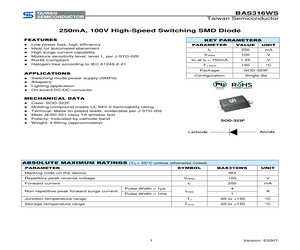
BAS316WS Taiwan Semiconductor 250mA, 100V High-Speed Switching SMD Diode FEATURES KEY PARAMETERS Low power loss, high efficiency Ideal for automated placement High surge current capability Moisture sensitivity level: level 1, per J-STD-020 RoHS Compliant Halogen-free according to IEC 61249-2-21 PARAMETER VALUE UNIT IF 250 mA VRRM 100 V VF at IF = 150mA 1.25 V TJ MAX 150 C APPLICATIONS Switching mode power supply (SMPS) Adapters Lighting application On-board DC/DC converter Package SOD-323F Configuration Single die MECHANICAL DATA Case: SOD-323F Molding compound meets UL 94V-0 flammability rating Terminal: Matte tin plated leads, solderable per J-STD-002 Meet JESD 201 class 1A whisker test Polarity: Indicated by cathode band Weight: 4.60mg (approximately) SOD-323F ABSOLUTE MAXIMUM RATINGS (TA = 25C unless otherwise noted) PARAMETER SYMBOL Marking code on the device UNIT W2 Repetitive peak reverse voltage Forward current Non-repetitive peak forward surge current BAS316WS Pulse Width =
 5 Pages, 359 KB, Original
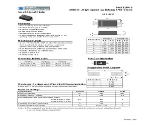
BAS316WS 200mW, High-speed switching SMD Diode Small Signal Diode SOD-323F Features Fast switching device(Trr<4.0nS) Surface device type mounting Moisture sensitivity level 1 Matte Tin(Sn) lead finish Pb free version, RoHS compliant Green compound (Halogen free) with suffix "G" on packing code and prefix "G" on date code Unit (mm) Dimensions Mechanical Data Unit (inch) Min Max Case : Flat lead SOD-323F small outline plastic package A 1.15 1.40 0.045 0.055 Min Max Terminal: Matte tin plated, lead free., solderable per MIL-STD-202, Method 208 guaranteed B 2.30 2.80 0.091 0.106 C 0.25 0.40 0.010 0.016 High temperature soldering guaranteed: 260C/10s D 1.60 1.80 0.063 0.071 Polarity : Indicated by cathode band E 0.80 1.10 0.031 0.043 Weight : 4.60.5 mg F 0.05 0.15 0.002 0.006 Marking Code : W2 Ordering Information Pin Configuration Part No. Package Packing BAS316WS RR SOD-323F 3Kpcs / 7" Reel BAS316WS RRG SOD-323F 3Kpcs / 7" Reel Suggested PAD Layout X1 Y(2X) X(2X) Dimensions
 4 Pages, 79 KB, Original
BAS316WS 200mW, High-speed switching SMD Diode Small Signal Diode SOD-323F Features Fast switching device(Trr<4.0nS) Surface device type mounting Moisture sensitivity level 1 Matte Tin(Sn) lead finish Pb free version, RoHS compliant Green compound (Halogen free) with suffix "G" on packing code and prefix "G" on date code Unit (mm) Dimensions Mechanical Data Unit (inch) Min Max Case : Flat lead SOD-323F small outline plastic package A 1.15 1.40 0.045 0.055 Min Max Terminal: Matte tin plated, lead free., solderable per MIL-STD-202, Method 208 guaranteed B 2.30 2.80 0.091 0.106 C 0.25 0.40 0.010 0.016 High temperature soldering guaranteed: 260C/10s D 1.60 1.80 0.063 0.071 Polarity : Indicated by cathode band E 0.80 1.10 0.031 0.043 Weight : 4.60.5 mg F 0.05 0.15 0.002 0.006 Marking Code : W2 Ordering Information Pin Configuration Part No. Package Packing BAS316WS RR SOD-323F 3Kpcs / 7" Reel BAS316WS RRG SOD-323F 3Kpcs / 7" Reel Suggested PAD Layout X1 Y(2X) X(2X) Dimensions
 3 Pages, 78 KB, Original
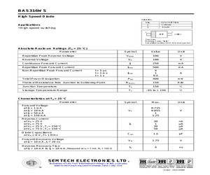
BAS316WS High Speed Switching Diode PINNING Applications * High-speed switching DESCRIPTION PIN 1 Cathode 2 Anode 2 1 W2 Top View Marking Code: "W2" Simplified outline SOD-323 and symbol Absolute Maximum Ratings (Ta = 25 OC) Parameter Symbol Value Unit VRRM 100 V Reverse Voltage VR 100 V Continuous Forward Current IF 250 mA IFRM 500 mA IFSM 4 1 0.5 A Ptot 200 mW Tj 150 O Tstg - 65 to + 150 O Symbol Max. Repetitive Peak Reverse Voltage Repetitive Peak Forward Current Non-Repetitive Peak Forward Current t = 1 s t = 1 ms t=1s Total Power Dissipation Junction Temperature Storage Temperature Range C C Characteristics at Ta = 25 OC Parameter Forward Voltage at IF = 1 mA at IF = 10 mA at IF = 50 mA at IF = 150 mA VF Reverse Current at VR = 25 V at VR = 75 V at VR = 25 V, TJ = 150 OC at VR = 75 V, TJ = 150 OC IR Diode Capacitance at VR = 0 V, f = 1 MHz Reverse Recovery Time at IF = IR = 10 mA, Irr = 0.1 X IR , RL = 100 0.715 0.855 1 1.25 Unit V 30 1 30 50 nA A A A Ctot 1.5 pF trr 4 ns SEMTECH ELECTRONICS
 3 Pages, 301 KB, Original
BAS316WS High Speed Diode PINNING DESCRIPTION PIN Applications * High-speed switching 1 Cathode 2 Anode 2 1 WD Top View Marking Code: "WD" Simplified outline SOD-323 and symbol Absolute Maximum Ratings (Ta = 25 OC) Parameter Symbol Value Unit VRRM 100 V Reverse Voltage VR 100 V Continuous Forward Current IF 250 mA IFRM 500 mA IFSM 4 1 0.5 A Ptot 400 mW Rth(j-s) 150 K/W Junction Temperature TJ 150 O Storage Temperature Range Ts - 65 to + 150 O Symbol Max. Repetitive Peak Reverse Voltage Repetitive Peak Forward Current Non-Repetitive Peak Forward Current t = 1 s t = 1 ms t=1s Total Power Dissipation Thermal Resistance from Junction to Soldering Point C C Characteristics at Ta = 25 OC Parameter Forward Voltage at IF = 1 mA at IF = 10 mA at IF = 50 mA at IF = 150 mA VF Reverse Current at VR = 25 V at VR = 75 V at VR = 25 V, TJ = 150 OC at VR = 75 V, TJ = 150 OC IR 0.715 0.855 1 1.25 Unit V 30 1 30 50 nA A A A Diode Capacitance at VR = 0 V, f = 1 MHz Ctot 1.5 pF Forward Recovery Voltage at IF = 10 mA,
 3 Pages, 195 KB, Original
BAS316WS High Speed Diode PINNING DESCRIPTION PIN Applications * High-speed switching 1 Cathode 2 Anode 2 1 WD Top View Marking Code: "WD" Simplified outline SOD-323 and symbol Absolute Maximum Ratings (Ta = 25 OC) Parameter Symbol Value Unit VRRM 100 V Reverse Voltage VR 100 V Continuous Forward Current IF 250 mA IFRM 500 mA IFSM 4 1 0.5 A Total Power Dissipation Ptot 400 mW Junction Temperature TJ 150 O Storage Temperature Range Ts - 65 to + 150 O Symbol Max. Repetitive Peak Reverse Voltage Repetitive Peak Forward Current Non-Repetitive Peak Forward Current t = 1 s t = 1 ms t=1s C C Characteristics at Ta = 25 OC Parameter Forward Voltage at IF = 1 mA at IF = 10 mA at IF = 50 mA at IF = 150 mA VF Reverse Current at VR = 25 V at VR = 75 V at VR = 25 V, TJ = 150 OC at VR = 75 V, TJ = 150 OC IR 0.715 0.855 1 1.25 Unit V 30 1 30 50 nA A A A Diode Capacitance at VR = 0 V, f = 1 MHz Ctot 1.5 pF Forward Recovery Voltage at IF = 10 mA, tr = 20 ns Vfr 1.75 V Reverse Recovery Time at IF = 10 mA to IR = 10
 3 Pages, 197 KB, Original
5 137 BAS116 28 3.0SMCJ11 to 3.0SMCJ220A 175-176 BAS15 26 3.0SMCJ11C to 3.0SMCJ220CA 175-176 BAS16 28 30DF6 46 BAS16WS 27 30KP Series 191-192 BAS19 to BAS21 28 31DQ03 to 31DQ10 64 BAS216WS 27 3EZ3.9D10 to 3EZ200D10 141 BAS216WT 28 3EZ3.9D5 to 3EZ200D5 141 BAS316WS 27 3JH45 46 BAS321 27 3KE Series 177-178 BAS40/04/ 05/ 06 73 3TH41 32 BAS40W/04W/ 05W/ 06W 73 5KP Series 179-180 BAS521 28 6A05 to 6A10 20 BAS70-00 to BAS70-06 29 ABR1000 to ABR1010 220 BAS81 to BAS83 70 5 Numerical Index Type No. Page Type No. Page BAS85 to BAS86 69 BY133 14 BAT400D 73 BY133G 22 BAT41 to BAT48 69 BY251 to BY255 20 BAT42W to BAT43W 71 BY296 to BY299 45 BAT42WS 71 BY396 to BY399 45 BAT42WS to BAT43WS 71 BY550-50 to BY550-1000 20 BAT42WT 71 BY8004 to BY8006 32 BAT43WS 71 BYD13D to BYD13M 35 BAT43WT 71 BYD17D to BYD17M 35 BAT46W 71 BYD33D to BYD33M 36 BAT54 Series. 73 BYD37D to BYD37M 37 BAT54W 71 BYD37DA to BYD37MA 37 BAT54WS 71 BYD57D to BYD57V 37 BAT54WT 71 BYD77A to BYD77G 38 BAT81 to BAT86 69 BYG10D to BYG10M 36 BAV10
 244 Pages, 3329 KB, Original
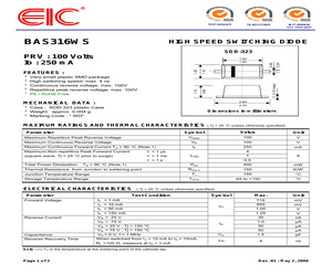
BAS316WS TW00/17276EM IATF 0060636 SGS TH07/1033 HIGH SPEED SWITCHING DIODE PRV : 100 Volts Io : 250 mA 0.40 0.15 (max) 1.15 Very small plastic SMD package High switching speed: max. 4 ns Continuous reverse voltage: max. 100V Repetitive peak reverse voltage: max. 100V Pb / RoHS Free 0.80 * * * * * 1.35 FEATURES : 1.10 1.80 1.60 0.25 SOD-323 2.80 MECHANICAL DATA : 2.30 * Case : SOD-323 plastic Case * Weight : approx. 0.004 g * Marking Code : " WD" Dimensions in millimeters MAXIMUM RATINGS AND THERMAL CHARACTERISTICS ( Tj = 25 C unless otherwise specified) Symbol Value Unit VRRM 100 V Maximum Continuous Reverse Voltage VR 100 V Maximum Continuous Forward Current T S = 90 C (Note 1) IF 250 mA IFSM 4 1 0.5 A Parameter Maximum Repetitive Peak Reverse Voltage Maximum Non-repetitive Peak Forward Current (square wave; Tj = 25 C prior to surge) Total Power Dissipation t = 1 s t = 1 ms t =1s T S = 90 C (Note 1) Ptot 400 mW Rth(j-s) 150 K/W Junction Temperature Range TJ 150 C Storage Temperature Range TSTG
 2 Pages, 92 KB, Original


