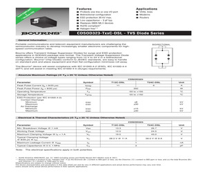
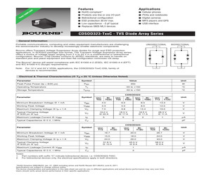
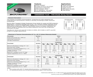
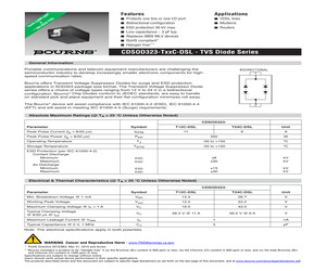
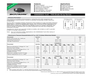
res Applications Low leakage current: 1 nA Communication lines Bidirectional configuration Portable electronics ESD protection 30 kV max. Low capacitance: 3 pF typ. Replaces 0805 MLV devices RoHS compliant* and halogen free** AEC-Q101 compliant product*** CDSOD323-T24C-DSLQ - TVS Diode Series General Information Portable communications and telecom equipment manufacturers are challenging the semiconductor industry to develop increasingly smaller electronic components for highspeed communication rates. BIDIRECTIONAL 1 Bourns offers Transient Voltage Suppressor Diodes for surge and ESD protection applications in SOD323 package size format. Bourns(R) Chip Diodes conform to JEDEC The Bourns(R) device will assist compliance with IEC 61000-4-2 (ESD), IEC 61000-4-4 (EFT) and IEC 61000-4-5 (Surge) requirements. 2 Absolute Maximum Ratings (@ TA = 25 C Unless Otherwise Noted) Parameter Symbol Peak Pulse Current (tp = 8/20 s) CDSOD323-T24C-DSLQ Unit IPPM 6 A TJ -55 to +150 C TSTG -55 to +150 C E
 5 Pages, 286 KB, Original
.........................................................................1 CDSOD323-T18C..........................................................................1C CDSOD323-T24 ............................................................................4 CDSOD323-T24C..........................................................................4C Specifications are subject to change without notice. The device characteristics and parameters in this data sheet can and do vary in different applications and actual device performance may vary over time. Users should verify actual device performance in their specific applications. CDSOD323-TxxC - TVS Diode Array Series Performance Graphs Peak Pulse Power vs Pulse Time Pulse Waveform 120 1,000 350 W, 8/20 s Waveform 100 10 0.1 IPP - Peak Pulse Current (% of IPP) PPP - Peak Pulse Current (W) 10,000 Test Waveform Parameters tt = 8 s td = 20 s tt 100 80 et 60 40 td = t|IPP/2 20 0 1 10 100 1,000 10,000 0 5 10 Block Diagram 15 20 25 30 t - Time (s) td - Pulse D
 5 Pages, 273 KB, Original
06) D 0.92 - 1.14 (0.036 - 0.045) E 0.25 - 0.40 (0.010 - 0.016) F 0.08 - 0.20 (0.003 - 0.008) Each device has device marking outlined below. H 0.13 ......... (0.005) MAX. CDSOD323-T12C-DSL ............................................................... 2D CDSOD323-T24C-DSL ................................................................ 4D DIMENSIONS: DIMENSIONS: MM (INCHES) Typical Part Marking MM (INCHES) Specifications are subject to change without notice. The device characteristics and parameters in this data sheet can and do vary in different applications and actual device performance may vary over time. Users should verify actual device performance in their specific applications. CDSOD323-TxxC-DSL - TVS Diode Series Packaging Information The surface mount product is packaged in an 8 mm x 4 mm tape and reel format per EIA-481 standard. P 0 P 1 d T E Index Hole 120 F D2 W B D1 D P A Trailer ....... ....... End C Device ....... ....... ....... ....... Leader ....... ....... W1 Start DIMENSIONS
 5 Pages, 281 KB, Original
323-T18 ........................................................................1 CDSOD323-T18C ......................................................................1C CDSOD323-T24 ........................................................................4 CDSOD323-T24C ......................................................................4C CDSOD323-TxxC - TVS Diode Array Series Packaging Information The surface mount product is packaged in an 8 mm x 4 mm tape and reel format per EIA-481 standard. P 0 P 1 d T E Index Hole 120 F D2 W B D1 D P A Trailer C Device Leader ....... ....... ....... ....... ....... ....... ....... ....... End 10 pitches (min.) W1 Start 10 pitches (min.) Direction of Feed Item Symbol Carrier Width A Carrier Length B Carrier Depth C Sprocket Hole d Reel Outside Diameter D Reel Inner Diameter D1 Feed Hole Diameter D2 Sprocket Hole Position E Punch Hole Position F Punch Hole Pitch P Sprocket Hole Pitch P0 Embossment Center P1 Overall Tape Thickness T Tape Width W Reel Width W
 4 Pages, 227 KB, Original
323-T18 ........................................................................1 CDSOD323-T18C ......................................................................1C CDSOD323-T24 ........................................................................4 CDSOD323-T24C ......................................................................4C CDSOD323-TxxC - TVS Diode Series Packaging Information The surface mount product is packaged in an 8 mm x 4 mm tape and reel format per EIA-481 standard. P 0 P 1 d T E Index Hole 120 F D2 W B D1 D P A Trailer C Device Leader ....... ....... ....... ....... ....... ....... ....... ....... End 10 pitches (min.) W1 Start 10 pitches (min.) Direction of Feed Item Symbol Carrier Width A Carrier Length B Carrier Depth C Sprocket Hole d Reel Outside Diameter D Reel Inner Diameter D1 Feed Hole Diameter D2 Sprocket Hole Position E Punch Hole Position F Punch Hole Pitch P Sprocket Hole Pitch P0 Embossment Center P1 Overall Tape Thickness T Tape Width W Reel Width W1 Quan
 4 Pages, 221 KB, Original
06) D 0.92 - 1.14 (0.036 - 0.045) E 0.25 - 0.40 (0.010 - 0.016) F 0.08 - 0.20 (0.003 - 0.008) Each device has device marking outlined below. H 0.13 ......... (0.005) MAX. CDSOD323-T12C-DSL ............................................................... 2D CDSOD323-T24C-DSL ................................................................ 4D DIMENSIONS: DIMENSIONS: MM (INCHES) Typical Part Marking MM (INCHES) Specifications are subject to change without notice. The device characteristics and parameters in this data sheet can and do vary in different applications and actual device performance may vary over time. Users should verify actual device performance in their specific applications. CDSOD323-TxxC-DSL - TVS Diode Series Packaging Information The surface mount product is packaged in an 8 mm x 4 mm tape and reel format per EIA-481 standard. P 0 P 1 d T E Index Hole 120 F D2 W B D1 D P A Trailer ....... ....... End C Device ....... ....... ....... ....... Leader ....... ....... W1 Start DIMENSIONS
 4 Pages, 265 KB, Original
.........................................................................1 CDSOD323-T18C..........................................................................1C CDSOD323-T24 ............................................................................4 CDSOD323-T24C..........................................................................4C Specifications are subject to change without notice. The device characteristics and parameters in this data sheet can and do vary in different applications and actual device performance may vary over time. Users should verify actual device performance in their specific applications. CDSOD323-TxxC - TVS Diode Array Series Performance Graphs Peak Pulse Power vs Pulse Time Pulse Waveform 120 1,000 350 W, 8/20 s Waveform 100 10 0.1 IPP - Peak Pulse Current (% of IPP) PPP - Peak Pulse Current (W) 10,000 Test Waveform Parameters tt = 8 s td = 20 s tt 100 80 et 60 40 td = t|IPP/2 20 0 1 10 100 1,000 10,000 0 5 10 Block Diagram 15 20 25 30 t - Time (s) td - Pulse D
 4 Pages, 264 KB, Original
1 Discrete Low Capacitance Transient Voltage Suppressor (TVS) Diodes Part Number CDSOD323-T03 CDSOD323-T05 CDSOD323-T08 CDSOD323-T12 CDSOD323-T15 CDSOD323-T18 CDSOD323-T24 CDSOD323-T03C CDSOD323-T05C CDSOD323-T08C CDSOD323-T12C CDSOD323-T15C CDSOD323-T18C CDSOD323-T24C Pkg. Size SOD-323 SOD-323 SOD-323 SOD-323 SOD-323 SOD-323 SOD-323 SOD-323 SOD-323 SOD-323 SOD-323 SOD-323 SOD-323 SOD-323 Vrwm (V) Vrsm (V) Irsm (A) 3.3 5 8 12 15 18 24 3.3 5 8 12 15 18 24 19 18.3 18.5 28.3 31.8 45 56 19 18.3 18.5 28.3 31.8 45 56 20 17 17 11 10 8 6 20 17 17 11 10 8 6 Electrical Characterization (Ta = 25 C) Ppk Vbr min. @ If Ct Typ (W) (V) (mA) (pF) 5 350 350 350 350 350 350 350 350 350 350 350 350 350 350 4 6 8.5 13.3 16.7 20 26.7 4 6 8.5 13.3 16.7 20 26.7 1 1 1 1 1 1 1 1 1 1 1 1 1 1 3 3 3 3 3 3 3 3 3 3 3 3 3 3 @ Vr (V) @F (MHz) 0 0 0 0 0 0 0 0 0 0 0 0 0 0 1 1 1 1 1 1 1 1 1 1 1 1 1 1 Discrete 400W Transient Voltage Suppressor (TVS) Diodes Electrical Characterization (Ta = 25 C) Ppk Vrsm Irsm Vbr min. (V) (A) (V) (W
 16 Pages, 885 KB, Original
5-100-WH) 2031-23T-SM CDSOD323-T05LC (2015-23-xxx) SDI TxRING RxTIP 2031-42T-SM 1 RRING Fuse 1.25 A RxRING RS232 Interface Intelligent Transport System TBU-CA065-100-WH (TBU-CA085-100-WH) RS232 TBU-CA065-200-WH (TBU-CA085-100-WH) 2031-23T-SM (2015-23-xxx) CDSOD323-T24C 75 RS422 Interface 2031-23T-SM (2015-23-xxx) Microwave Link TBU-CA065-100-WH CDSOD323-T12C MOV-10D201K RS422 75 Coax Composite Video TBU-CA025-300-WH HV LP Filter DC or AC Power IF TX/RX 2031-15T-SM Protection for higher power split-mounted infrared feed equipment 6 Ethernet Surge and Power Cross Protection - GR-1089 ISSUE 6, Port Type 4 RS485 Interface TBU-CA065-300-WH CDSOT23-SM712 MOV-10D201K 1 CT : 1 CT RS485 2031-23T-SM-RPLF Not Used To Connector Ethernet PHY 2031-23T-SM-RPLF 1/4 SM51589L TBU-DT065-300-WH MOV-10D201K Ethernet Protection Circuit Test Results - Differential Surge Test: 800 V, 1.2/50 s Voltage, 8/20 s Current TBU(R) HSP Current (2 A/DIV) Ch1 Max 552 V 3 Total Surge Current (50 A/DIV) 4 Ch1 Max 510 V Ch3 Max 2.12
 12 Pages, 2422 KB, Original
F 0.08 - 0.20 (0.003 - 0.008) H 0.13 (0.005) MAX. ......... J 0.30 - 0.45 (0.012 - 0.018) DIMENSIONS: Typical Part Marking Each device has device marking outlined below. CDSOD323-T12C-DSL ................................................................ 2D CDSOD323-T24C-DSL................................................................. 4D MM (INCHES) Specifications are subject to change without notice. The device characteristics and parameters in this data sheet can and do vary in different applications and actual device performance may vary over time. Users should verify actual device performance in their specific applications. CDSOD323-TxxC-DSL - TVS Diode Series Packaging Information The surface mount product is packaged in an 8 mm x 4 mm tape and reel format per EIA-481 standard. P 0 P 1 d T E Index Hole 120 F D2 W B D1 D P A Trailer ....... ....... End C Device ....... ....... 10 pitches (min.) ....... ....... Leader ....... ....... Symbol SOD-323 Carrier Width A 1.55 0.10 (0.061 0.004) Car
 4 Pages, 340 KB, Original
.........................................................................1 CDSOD323-T18C..........................................................................1C CDSOD323-T24.............................................................................4 CDSOD323-T24C..........................................................................4C Environmental Specifications Moisture Sensitivity Level.................................................................1 ESD Classification (HBM)............................................................. 3B Specifications are subject to change without notice. The device characteristics and parameters in this data sheet can and do vary in different applications and actual device performance may vary over time. Users should verify actual device performance in their specific applications. CDSOD323-TxxC - TVS Diode Array Series Performance Graphs Peak Pulse Power vs Pulse Time Pulse Waveform 120 1,000 350 W, 8/20 s Waveform 100 10 0.1 1 10 100 1,000 10,000
 4 Pages, 367 KB, Original
.........................................................................1 CDSOD323-T18C..........................................................................1C CDSOD323-T24 ............................................................................4 CDSOD323-T24C..........................................................................4C Specifications are subject to change without notice. Customers should verify actual device performance in their specific applications. CDSOD323-TxxC - TVS Diode Array Series Performance Graphs Peak Pulse Power vs Pulse Time Pulse Waveform 120 1,000 350 W, 8/20 s Waveform 100 10 0.1 IPP - Peak Pulse Current (% of IPP) PPP - Peak Pulse Current (W) 10,000 Test Waveform Parameters tt = 8 s td = 20 s tt 100 80 et 60 40 td = t|IPP/2 20 0 1 10 100 1,000 10,000 0 5 10 Block Diagram 15 20 25 30 t - Time (s) td - Pulse Duration (s) How to Order UNIDIRECTIONAL 1 BIDIRECTIONAL 1 CD SOD323 - T 05 C Common Code Chip Diode Package SOD323 = SOD-323 Package Model T = Transi
 4 Pages, 262 KB, Original
.........................................................................1 CDSOD323-T18C..........................................................................1C CDSOD323-T24 ............................................................................4 CDSOD323-T24C..........................................................................4C Specifications are subject to change without notice. The device characteristics and parameters in this data sheet can and do vary in different applications and actual device performance may vary over time. Users should verify actual device performance in their specific applications. CDSOD323-TxxC - TVS Diode Array Series Performance Graphs Peak Pulse Power vs Pulse Time Pulse Waveform 120 1,000 350 W, 8/20 s Waveform 100 10 0.1 IPP - Peak Pulse Current (% of IPP) PPP - Peak Pulse Current (W) 10,000 Test Waveform Parameters tt = 8 s td = 20 s tt 100 80 et 60 40 td = t|IPP/2 20 0 1 10 100 1,000 10,000 0 5 10 Block Diagram 15 20 25 30 t - Time (s) td - Pulse D
 4 Pages, 253 KB, Original
 F 0.08 - 0.20 (0.003 - 0.008) H 0.13 ......... (0.005) MAX. J 0.30 - 0.45 (0.012 - 0.018) DIMENSIONS: Typical Part Marking Each device has device marking outlined below. CDSOD323-T12C-DSL ............................................................... 2D CDSOD323-T24C-DSL ................................................................ 4D MM (INCHES) Specifications are subject to change without notice. Users should verify actual device performance in their specific applications. The products described herein and this document are subject to specific legal disclaimers as set forth on the last page of this document, and at www.bourns.com/docs/legal/disclaimer.pdf. CDSOD323-TxxC-DSL - TVS Diode Series Packaging Information The surface mount product is packaged in an 8 mm x 4 mm tape and reel format per EIA-481 standard. P 0 P 1 d T E Index Hole 120 F D2 W B D1 D P A Trailer ....... ....... End C Device ....... ....... 10 pitches (min.) ....... ....... Leader ....... ....... Symbol SOD-323 Carrier W
 5 Pages, 168 KB, Original
.........................................................................1 CDSOD323-T18C..........................................................................1C CDSOD323-T24 ............................................................................4 CDSOD323-T24C..........................................................................4C Specifications are subject to change without notice. Customers should verify actual device performance in their specific applications. CDSOD323-TxxC - TVS Diode Array Series Performance Graphs Peak Pulse Power vs Pulse Time Pulse Waveform 120 1,000 350 W, 8/20 s Waveform 100 10 0.1 IPP - Peak Pulse Current (% of IPP) PPP - Peak Pulse Current (W) 10,000 Test Waveform Parameters tt = 8 s td = 20 s tt 100 80 et 60 40 td = t|IPP/2 20 0 1 10 100 1,000 10,000 0 5 10 Block Diagram 15 20 25 30 t - Time (s) td - Pulse Duration (s) How to Order UNIDIRECTIONAL 1 BIDIRECTIONAL 1 CD SOD323 - T 05 C Common Code Chip Diode Package SOD323 = SOD-323 Package Model T = Transi
 4 Pages, 251 KB, Original


