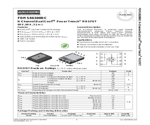
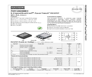
FDMS86300DC N-Channel Dual CoolTM Power Trench(R) MOSFET 80 V, 60 A, 3.1 m Features Dual CoolTM General Description Top Side Cooling PQFN package This N-Channel MOSFET is produced using Fairchild Semiconductor's advanced Power Trench(R) process. Advancements in both silicon and Dual CoolTM package technologies have been combined to offer the lowest rDS(on) while maintaining excellent switching performance by extremely low Junction-to-Ambient thermal resistance. Max rDS(on) = 3.1 m at VGS = 10 V, ID = 24 A Max rDS(on) = 4.0 m at VGS = 8 V, ID = 21 A High performance technology for extremely low rDS(on) 100% UIL Tested Applications RoHS Compliant Synchronous Rectifier for DC/DC Converters Telecom Secondary Side Rectification High End Server/Workstation Vcore Low Side D D D S Pin 1 S D S D S D G D D G Top S S Pin 1 S Bottom Power 56 MOSFET Maximum Ratings TA = 25 C unless otherwise noted Symbol VDS Drain to Source Voltage Parameter VGS Gate to Source Voltage Drain Current -Continuous (Package limite
 8 Pages, 266 KB, Original
ating and Storage Junction Temperature Range 2.5 -55 to +150 A mJ W C Thermal Characteristics RJC Thermal Resistance, Junction to Case RJA Thermal Resistance, Junction to Ambient 1.2 (Note 1a) 50 C/W Package Marking and Ordering Information Device Marking FDMS86300 Device FDMS86300 (c)2012 Fairchild Semiconductor Corporation FDMS86300 Rev.C1 Package Power 56 1 Reel Size 13 '' Tape Width 12 mm Quantity 3000 units www.fairchildsemi.com FDMS86300 N-Channel PowerTrench(R) MOSFET October 2012 FDMS86300 Symbol Parameter Test Conditions Min Typ Max Units Off Characteristics BVDSS Drain to Source Breakdown Voltage ID = 250 A, VGS = 0 V BVDSS TJ Breakdown Voltage Temperature Coefficient ID = 250 A, referenced to 25 C IDSS Zero Gate Voltage Drain Current VDS = 64 V, VGS = 0 V 1 A IGSS Gate to Source Leakage Current VGS = 20 V, VDS = 0 V 100 nA 4.5 V 80 V 39 mV/C On Characteristics VGS(th) Gate to Source Threshold Voltage VGS = VDS, ID = 250 A VGS(th) TJ G
 7 Pages, 300 KB, Original
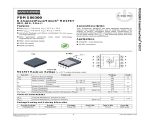
FDMS86300DC N-Channel Dual CoolTM 56 PowerTrench(R) MOSFET 80 V, 110 A, 3.1 m Features Dual CoolTM General Description Top Side Cooling PQFN package This N-Channel MOSFET is produced using Fairchild Semiconductor's advanced PowerTrench(R) process. Advancements in both silicon and Dual CoolTM package technologies have been combined to offer the lowest rDS(on) while maintaining excellent switching performance by extremely low Junction-to-Ambient thermal resistance. Max rDS(on) = 3.1 m at VGS = 10 V, ID = 24 A Max rDS(on) = 4.0 m at VGS = 8 V, ID = 21 A High performance technology for extremely low rDS(on) 100% UIL Tested Applications RoHS Compliant Synchronous Rectifier for DC/DC Converters Telecom Secondary Side Rectification High End Server/Workstation Vcore Low Side D D D S Pin 1 S D S D S D G D D G Top Dual Cool TM S S Pin 1 S Bottom 56 MOSFET Maximum Ratings TA = 25 C unless otherwise noted Symbol VDS Drain to Source Voltage Parameter VGS Gate to Source Voltage Drain Current -Continuous TC = 2
 9 Pages, 297 KB, Original
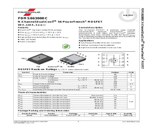
FDMS86300DC N-Channel Dual CoolTM Power Trench(R) MOSFET 80 V, 76 A, 3.1 m Features Dual CoolTM General Description Top Side Cooling PQFN package This N-Channel MOSFET is produced using Fairchild Semiconductor's advanced Power Trench(R) process. Advancements in both silicon and Dual CoolTM package technologies have been combined to offer the lowest rDS(on) while maintaining excellent switching performance by extremely low Junction-to-Ambient thermal resistance. Max rDS(on) = 3.1 m at VGS = 10 V, ID = 24 A Max rDS(on) = 4.0 m at VGS = 8 V, ID = 21 A High performance technology for extremely low rDS(on) 100% UIL Tested Applications RoHS Compliant Synchronous Rectifier for DC/DC Converters Telecom Secondary Side Rectification High End Server/Workstation Vcore Low Side D D D S Pin 1 S D S D S D G D D G Top S S Pin 1 S Bottom Power 56 MOSFET Maximum Ratings TA = 25 C unless otherwise noted Symbol VDS Drain to Source Voltage Parameter Ratings 80 VGS Gate to Source Voltage ID Drain Current -Continuous T
 8 Pages, 392 KB, Original
erating and Storage Junction Temperature Range 2.5 -55 to +150 mJ W C Thermal Characteristics RJC Thermal Resistance, Junction to Case RJA Thermal Resistance, Junction to Ambient 1.2 (Note 1a) 50 C/W Package Marking and Ordering Information Device Marking FDMS86300 Device FDMS86300 (c)2011 Fairchild Semiconductor Corporation FDMS86300 Rev.C Package Power 56 1 Reel Size 13 '' Tape Width 12 mm Quantity 3000 units www.fairchildsemi.com FDMS86300 N-Channel PowerTrench(R) MOSFET August 2011 FDMS86300 Symbol Parameter Test Conditions Min Typ Max Units Off Characteristics BVDSS Drain to Source Breakdown Voltage ID = 250 A, VGS = 0 V BVDSS TJ Breakdown Voltage Temperature Coefficient ID = 250 A, referenced to 25 C IDSS Zero Gate Voltage Drain Current VDS = 64 V, VGS = 0 V 1 A IGSS Gate to Source Leakage Current VGS = 20 V, VDS = 0 V 100 nA 4.5 V 80 V 39 mV/C On Characteristics VGS(th) Gate to Source Threshold Voltage VGS = VDS, ID = 250 A VGS(th) TJ Gat
 7 Pages, 196 KB, Original
ges that ON Semiconductor was negligent regarding the design or manufacture of the part. ON Semiconductor is an Equal Opportunity/Affirmative Action Employer. This literature is subject to all applicable copyright laws and is not for resale in any manner. FDMS86300 N-Channel PowerTrench(R) MOSFET 80 V, 122 A, 3.9 m Features General Description Max rDS(on) = 3.9 m at VGS = 10 V, ID = 19 A This N-Channel MOSFET has been designed specifically to improve the overall efficiency and to minimize switch node ringing of DC/DC converters using either synchronous or conventional switching PWM controllers.It has been optimized for low gate charge, low rDS(on), fast switching speed and body diode reverse recovery performance. Max rDS(on) = 5.5 m at VGS = 8 V, ID = 15.5 A Advanced Package and Silicon combination for low rDS(on) and high efficiency Next generation enhanced engineered for soft recovery body diode technology, Applications MSL1 robust package design OringFET / Load Switching 100% UIL tested DC-DC
 9 Pages, 514 KB, Original
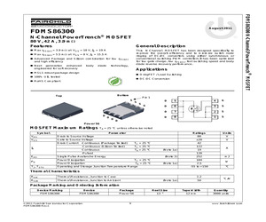
FDMS86300DC N-Channel Dual CoolTM Power Trench(R) MOSFET 80 V, 76 A, 3.1 m Features Dual CoolTM General Description Top Side Cooling PQFN package This N-Channel MOSFET is produced using Fairchild Semiconductor's advanced Power Trench(R) process. Advancements in both silicon and Dual CoolTM package technologies have been combined to offer the lowest rDS(on) while maintaining excellent switching performance by extremely low Junction-to-Ambient thermal resistance. Max rDS(on) = 3.1 m at VGS = 10 V, ID = 24 A Max rDS(on) = 4.0 m at VGS = 8 V, ID = 21 A High performance technology for extremely low rDS(on) 100% UIL Tested Applications RoHS Compliant Synchronous Rectifier for DC/DC Converters Telecom Secondary Side Rectification High End Server/Workstation Vcore Low Side D D D S Pin 1 S D S D S D G D D G Top S S Pin 1 S Bottom Power 56 MOSFET Maximum Ratings TA = 25 C unless otherwise noted Symbol VDS Drain to Source Voltage Parameter Ratings 80 VGS Gate to Source Voltage ID Drain Current -Continuous T
 8 Pages, 267 KB, Original
ges that ON Semiconductor was negligent regarding the design or manufacture of the part. ON Semiconductor is an Equal Opportunity/Affirmative Action Employer. This literature is subject to all applicable copyright laws and is not for resale in any manner. FDMS86300DC N-Channel Dual CoolTM 56 PowerTrench(R) MOSFET 80 V, 110 A, 3.1 m Features Dual CoolTM General Description Top Side Cooling PQFN package This N-Channel MOSFET is produced using Fairchild Semiconductor's advanced PowerTrench(R) process. Advancements in both silicon and Dual CoolTM package technologies have been combined to offer the lowest rDS(on) while maintaining excellent switching performance by extremely low Junction-to-Ambient thermal resistance. Max rDS(on) = 3.1 m at VGS = 10 V, ID = 24 A Max rDS(on) = 4.0 m at VGS = 8 V, ID = 21 A High performance technology for extremely low rDS(on) 100% UIL Tested Applications RoHS Compliant Synchronous Rectifier for DC/DC Converters Telecom Secondary Side Rectification High End Server/Work
 9 Pages, 341 KB, Original
ges that ON Semiconductor was negligent regarding the design or manufacture of the part. ON Semiconductor is an Equal Opportunity/Affirmative Action Employer. This literature is subject to all applicable copyright laws and is not for resale in any manner. FDMS86300 N-Channel PowerTrench(R) MOSFET 80 V, 122 A, 3.9 m Features General Description Max rDS(on) = 3.9 m at VGS = 10 V, ID = 19 A This N-Channel MOSFET has been designed specifically to improve the overall efficiency and to minimize switch node ringing of DC/DC converters using either synchronous or conventional switching PWM controllers.It has been optimized for low gate charge, low rDS(on), fast switching speed and body diode reverse recovery performance. Max rDS(on) = 5.5 m at VGS = 8 V, ID = 15.5 A Advanced Package and Silicon combination for low rDS(on) and high efficiency Next generation enhanced engineered for soft recovery body diode technology, Applications MSL1 robust package design OringFET / Load Switching 100% UIL tested DC-DC
 8 Pages, 455 KB, Original
ges that ON Semiconductor was negligent regarding the design or manufacture of the part. ON Semiconductor is an Equal Opportunity/Affirmative Action Employer. This literature is subject to all applicable copyright laws and is not for resale in any manner. FDMS86300 N-Channel PowerTrench(R) MOSFET 80 V, 122 A, 3.9 m Features General Description Max rDS(on) = 3.9 m at VGS = 10 V, ID = 19 A This N-Channel MOSFET has been designed specifically to improve the overall efficiency and to minimize switch node ringing of DC/DC converters using either synchronous or conventional switching PWM controllers.It has been optimized for low gate charge, low rDS(on), fast switching speed and body diode reverse recovery performance. Max rDS(on) = 5.5 m at VGS = 8 V, ID = 15.5 A Advanced Package and Silicon combination for low rDS(on) and high efficiency Next generation enhanced engineered for soft recovery body diode technology, Applications MSL1 robust package design OringFET / Load Switching 100% UIL tested DC-DC
 8 Pages, 466 KB, Original
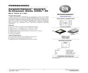
FDMS86300DC POWERTRENCH) MOSFET, N-Channel, DUAL COOL) 56 80 V, 110 A, 3.1 mW General Description www.onsemi.com This N-Channel MOSFET is produced using Fairchild Semiconductor's advanced POWERTRENCH(R) process that incorporates Shielded Gate technology. Advancements in both silicon and DUAL COOL(R) package technologies have been combined to offer the lowest rDS(on) while maintaining excellent switching performance by extremely low Junction-to-Ambient thermal resistance. ELECTRICAL CONNECTION Features * * * * * * DUAL COOL Top Side Cooling PQFN package Max rDS(on) = 3.1 mW at VGS = 10 V, ID = 24 A Max rDS(on) = 4.0 mW at VGS = 8 V, ID = 21 A High performance technology for extremely low rDS(on) 100% UIL Tested RoHS Compliant S D S D S D G D N-Channel MOSFET D D D D Pin 1 G S S Top Typical Applications S Pin 1 Bottom DFN8 5.1x6.15 (Dual Cool 56) CASE 506EG * Synchronous Rectifier for DC/DC Converters * Telecom Secondary Side Rectification * High End Server/Workstation Vcore Low Side MARKING DIAGRA
 8 Pages, 395 KB, Original
FDMS86300DC POWERTRENCH) MOSFET, N-Channel, DUAL COOL) 56 80 V, 110 A, 3.1 mW General Description www.onsemi.com This N-Channel MOSFET is produced using Fairchild Semiconductor's advanced POWERTRENCH(R) process that incorporates Shielded Gate technology. Advancements in both silicon and DUAL COOL(R) package technologies have been combined to offer the lowest rDS(on) while maintaining excellent switching performance by extremely low Junction-to-Ambient thermal resistance. ELECTRICAL CONNECTION Features * * * * * * DUAL COOL Top Side Cooling PQFN package Max rDS(on) = 3.1 mW at VGS = 10 V, ID = 24 A Max rDS(on) = 4.0 mW at VGS = 8 V, ID = 21 A High performance technology for extremely low rDS(on) 100% UIL Tested RoHS Compliant S D S D S D G D N-Channel MOSFET D D D D Pin 1 G S S Top Typical Applications S Pin 1 Bottom DFN8 5.1x6.15 (Dual Cool 56) CASE 506EG * Synchronous Rectifier for DC/DC Converters * Telecom Secondary Side Rectification * High End Server/Workstation Vcore Low Side MARKING DIAGRA
 8 Pages, 378 KB, Original
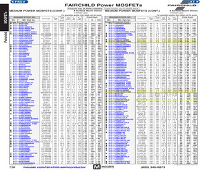
4N06 512-FDP025N06 512-FDBL0110N60 512-FDBL86561F085 512-FDP75N08A 512-FDP060AN08A0 512-FDB045AN08A0 512-FDP047N08 512-FDB031N08 512-FDA032N08 512-FDP023N08B_F102 512-FDC3512 512-FDS3590 512-FDS3580 512-FDMS3572 512-FDS3572 512-FDMC86320 512-FDMS86310 512-FDMS86300 512-FDMS86320 512-FDMD8280 512-FDD86326 512-FDMC86340ET80 512-FDMC86340 512-FDMS039N08B 512-FDMS86322 512-HUF75545S3ST 512-HUF75545P3 512-FDP86363_F085 512-FDB86360_F085 512-FDB86363_F085 512-FDMS86350ET80 512-FDP032N08B_F102 512-FDBL0150N80 512-FDBL86361F085 512-BSS123L 512-BSS123 512-FQT7N10LTF 512-FQT7N10TF 512-FDMA86108LZ 512-IRFM120ATF 512-FDC3612 512-FDT86106LZ 512-FDMA86151L 512-FDT86113LZ 512-FDT3612 512-FDD86113LZ 512-FDM3622 512-FDS3692 512-FQD7N10LTM 512-FDT86102LZ 512-FDD1600N10ALZD 512-FDS86141 512-FDMS86102LZ 512-FDMS3672 512-FDS3672 512-FDMC86106LZ 512-FQD13N10LTM 512-FQU13N10LTU 512-FDS86140 512-FDD86110 512-RFP12N10L 512-FQP13N10L 512-FQP13N10 512-FQD19N10LTM 512-FQD19N10TM 512-FDD850N10L 512-FDD850N10LD 512-FDMS86104
 1 Pages, 276 KB, Original
F095 SSOT-3 SSOT-3 512-FDN340P_F095 Power-33 512-FDMC610P SSOT-3 512-FDN306P_F095 Dual N-Channel SOIC-8 512-FDS8949 Power 33 512-FDMC8032L SSOT-6 512-NDC7002N SC-70 512-2N7002DW SOT-523F 512-2N7002V SOIC-8 512-FDS9945 Power-56 512-FDMS86500DC Power-56 512-FDMS86300DC SSOT-6 512-FDC3601N SSOT-6 512-FDC8602 512-FDS89161 SOIC-8 SOIC-8 512-FDS89141 SOIC-8 512-FDS3992 Power 3.3x5 512-FDMD82100 512-FDMS86101DC Power-56 Power 3.3x5 512-FDMD84100 Power-56 512-FDMD86100 Power-56 512-FDMD85100 Power-88 512-FDMT800152DC Power-88 512-FDMT800100DC Quad N-Channel MLP 4.5x5 512-FDMQ86530L Dual P-Channel SSOT-6 512-NDC7003P SOIC-8 512-NDS9948 512-FDS9958 TO-247 Complementary N & P Channel SOIC-8 512-FDS4897C 512-FDD8424H TO-252 VDS (V) RDS Qg ID (on) (nC) (A) (m) PD (W) Price Each 10 100 3.21 2.92 2.63 2.39 1.53 1.53 .96 .67 .80 .60 .92 3.05 2.16 1.04 .92 1.70 2.01 1.96 1.29 1.13 1.52 .92 .82 1.64 .59 .90 2.14 2.12 2.03 1.24 1.44 .91 .66 1.34 .85 .87 1.04 .67 .80 1.00 .77 .64 .99 .61 .51 .49 .48 .24 1.10 1.07 1.
 1 Pages, 280 KB, Original


