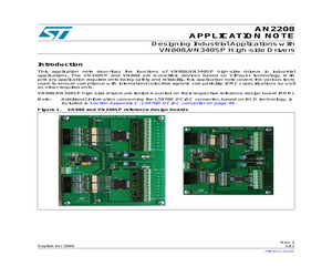
reference design board is assembled with uni-directional SM15TXXA Transil diodes because they protect the HSD against both positive and negative surge pulses. For more information about SM15TXXA Transil diodes from STMicroelectronics, please refer to the SM15T36A Datasheet available at www.st.com. Refer to Section A.2: Recommended VN808 PCB Layout on page 43 for more information about designing boards to improve EMC immunity and performance in industrial environments. 2.2 Surge suppression When designing your application, VCC and ground lines should lay on top of each other, minimizing the closed loop area and increasing the ability of the application to reject 9/51 AN2208 2 VN808 reference design board environmental noise. Figure 5 shows a surge suppression block using a uni-directional SM15T36A Transil diode. The Transil diode provides overvoltage protection for the HSD. The SM15T36A has a peak pulse power dissipation of 1500 W, stand-off voltage of 36 V and breakdown
 51 Pages, 2039 KB, Original
8 24 25.2 1 33.2 45 0.178 42.8 234 0.075 9.4 SM15T27A/CA 0.2 1 23.1 25.7 27 28.4 1 37.5 40 0.228 48.3 207 0.096 9.6 SM15T30A/CA 0.2 1 25.6 28.5 30 31.5 1 41.5 36 0.278 53.5 187 0.12 9.7 SM15T33A/CA 0.2 1 28.2 31.4 33 34.7 1 45.7 33 0.333 59.0 169 0.14 9.8 SM15T36A/CA 0.2 1 30.8 34.2 36 37.8 1 49.9 30 0.403 64.3 156 0.17 9.9 SM15T39A/CA 0.2 1 33.3 37.1 39 41.0 1 53.9 28 0.461 69.7 143 0.20 10.0 SM15T68A/CA 0.2 1 58.1 64.6 68 71.4 1 92 16.3 1.26 121 83 0.60 10.4 SM15T75A/CA 0.2 1 64.1 71.3 75 78.8 1 103 14.6 1.66 134 75 0.74 10.5 SM15T100A/CA 0.2 1 85.5 95.0 100 105 1 137 11 2.91 178 56 1.30 10.6 SM15T150A/CA 0.2 1 128 143 150 158 1 207 7.2 6.81 265 38 2.82 10.8 SM15T200A/CA 0.2 1 171 190 200 210 1 274 5.5 11.6 353 28 5.11 10.8 SM15T220A/CA 0.2 1 188 209 220 231 1 328 4.6 21.1 388 26 6.04 10.8 1. Pulse test : tp < 50 ms 2. To calculate VBR versus junction temperature, use the following formula: VBR @ TJ = VBR @ 25C x (1 + T x (TJ - 25)). 3. To calculate maximum clamping voltage at other surge level
 11 Pages, 115 KB, Original
 24 25.2 1 33.2 45 0.178 42.8 234 0.075 9.4 SM15T27AY/CAY 0.2 1 23.1 25.7 27 28.4 1 37.5 40 0.228 48.3 207 0.096 9.6 SM15T30AY/CAY 0.2 1 25.6 28.5 30 31.5 1 41.5 36 0.278 53.5 187 0.12 9.7 SM15T33AY/CAY 0.2 1 28.2 31.4 33 34.7 1 45.7 33 0.333 169 0.14 9.8 SM15T36AY/CAY 0.2 1 30.8 34.2 36 37.8 1 49.9 30 0.403 64.3 156 0.17 9.9 SM15T39AY/CAY 0.2 1 33.3 37.1 39 41.0 1 53.9 28 0.461 69.7 143 0.2 10 SM15T47AY/CAY 0.2 1 40.2 44.7 47 49.4 1 64.5 23.2 0.653 84 119 0.291 10.1 SM15T56AY/CAY 0.2 1 53.3 56 58.9 1 77.4 20 0.925 100 100 0.411 10.3 SM15T68AY/CAY 0.2 1 58.1 64.6 68 71.4 1 92 16.3 1.26 121 83 0.6 10.4 SM15T75AY/CAY 0.2 1 64.1 71.3 75 78.8 1 103 14.6 1.66 134 75 0.74 10.5 SM15T82AY/CAY 0.2 1 82 86.0 1 113 13.9 1.94 146 69 0.87 10.5 48 70 77.8 59 1. Pulse test: tp < 50 ms 2. To calculate maximum clamping voltage at other surge level, use the following formula: VCLmax = VCL - RD x (IPP - IPPappli) where IPPappli is the surge current in the application 3. To calculate VBR or VCL versus junction tempe
 13 Pages, 218 KB, Original
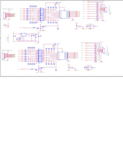
5 12 6 11 R23 20 INPUT15 1k5 GND_SIGNAL C22 10nF 37 U5 VCC VCC INPUT10 Vbss 6V J4 F2 FUSE J3 OUTPUT & POWER SUPPLY 24V CONNECTOR POINT POINT POINT POINT TP24 TP20 TP18 TP32 Output10 B HEADER 14 C GND_POWER L1 U9 7 2 3 8 1 2 3 4 5 6 7 8 9 10 11 12 13 14 D1 SM15T36A Vbss 6V L5970D Power Supply for DC/DC converter 8-35V + 4.7nF STATUS1 C C13 C1 22uF 50V Input 1 Input 2 Input 3 Input 4 Input 5 Input 6 Input 7 Input 8 Status Output Output Output Output Output Output Output Output Output Output Output Output Output Output Output Output 1 1 2 2 3 3 4 4 5 5 6 6 7 7 8 8 GND 36 35 34 33 32 31 30 29 28 27 26 25 24 23 22 21 Output9 Output13 Output10 C23 10nF Output11 Output12 1 2 3 4 5 6 7 8 9 10 B CONN PLUG 10 Output14 Output13 C24 10nF Output14 Output15 Output15 Output16 C25 10nF 19 VN808 Output16 R22 7 INPUT16 C26 10nF 10 GND_POWER_1 1k5 8 9 GND_POWER_1 GND_POWER_1 U7 TLP281-4 TP19 POINT TP22 TP23 TP34 TP25 POINT POINT POINT POINT TP26 POINT TP27 POINT TP29 POINT Input 24V DC1 VCC 24V_1 Vbss 6V C18 4.7nF
 1 Pages, 55 KB, Original
 10 F1 FUSE U2 GND_POW ER OUTPUT 4 VCC24V GND_SIGNAL Vbss_6V R9 R10 R11 R12 22k 22k 22k 22k GND_POW ER C4 10nF 1 6 R13 7k5 GND_POW ER 3 VCC24V 4 U3 TLP181 R14 STATUS1 J5 INPUT24V DC 1k 2 1 R11 1k5 CON2 GND_SIGNAL C5 100nF R16 C7 4k7 4.7nF + C6 22uF 50V D1 SM15T36A C8 D2 L-HLMP1700 4.7nF GND_POW ER GND_EARTH GND_POW ER GND_SIGNAL VCC24V INPUT 24V DC1 VCC24V1 U5 TLP281-4 J3 OUTPUT 5 VCC24V1 C11 10nF R18 INPUT 5 Vbss_6V 1 2 3 4 5 6 7 8 9 10 INPUT 5 INPUT 6 INPUT 7 INPUT 8 STATUS2 16 2 15 3 INPUT 6 4k7 14 4 13 5 12 6 11 R23 INPUT 7 7 8 4k7 9 R25 1k R26 7 1k 8 10 4k7 10 6 R27 9 GND_SIGNAL J5 VCC Output4 Input4 Output3 Input3 Output2 Input2 Output1 Input1 GND 4 OUTPUT 5 3 OUTPUT 6 2 OUTPUT 7 1 OUTPUT 8 Vbss_6V R28 R29 R30 R31 22k 22k 22k 22k C14 10nF C15 10nF OUTPUT 8 C16 10nF R32 330R VCC24V1 1 6 C19 100nF INPUT 24V DC1 3 4 U7 TLP181 + C20 22uF 50V R33 STATUS2 1k R35 1k5 4k7 C17 GND_POW ER1 4.7nF D5 L-HLMP1700 C18 4.7nF GND_EARTH GND_SIGNAL GND_POW ER1 GND_SIGNAL Vss Vbss_6V L5970D OUT VREF GND INH FB
 4 Pages, 130 KB, Original
 15 18 22 24 26 28 30 33 40 48 58 70 85 130 170 188 300 1000 500 10 5 5 5 5 5 5 5 5 5 5 5 5 5 5 5 800 800 500 5 5 1 1 1 1 1 1 1 1 1 1 1 1 1 1 1 1 1 SM5908 SM15T6V8A SM15T7V5A SM15T10A SM15T12A SM15T15A SM15T18A SM15T22A SM15T24A SM15T27A SM15T30A SM15T33A SM15T36A SM15T39A SM15T68A SM15T100A SM15T150A SM15T200A SM15T220A SMCJ5.0A-TR SMCJ6.0A-TR SMCJ6.5A-TR SMCJ10A-TR SMCJ12A-TR SMCJ13A-TR SMCJ15A-TR SMCJ18A-TR SMCJ22A-TR SMCJ24A-TR SMCJ26A-TR SMCJ28A-TR SMCJ30A-TR SMCJ33A-TR SMCJ40A-TR SMCJ48A-TR SMCJ58A-TR SMCJ70A-TR SMCJ85A-TR SMCJ130A-TR SMCJ170A-TR SMCJ188A-TR SM15T6V8CA SM15T7V5CA SM15T10CA SM15T12CA SM15T15CA SM15T18CA SM15T22CA SM15T24CA SM15T27CA SM15T30CA SM15T33CA SM15T36CA SM15T39CA SM15T68CA SM15T100CA SM15T150CA SM15T200CA SM15T220CA SMCJ5.0CA-TR SMCJ6.0CA-TR SMCJ6.5CA-TR SMCJ10CA-TR SMCJ12CA-TR SMCJ13CA-TR SMCJ15CA-TR SMCJ18CA-TR SMCJ22CA-TR SMCJ24CA-TR SMCJ26CA-TR SMCJ28CA-TR SMCJ30CA-TR SMCJ33CA-TR SMCJ40CA-TR SMCJ48CA-TR SMCJ58CA-TR SMCJ70CA-TR SMCJ85CA-TR SMCJ130CA-TR SMCJ170CA-
 48 Pages, 803 KB, Original
T & 6V OUTPUT CONNECTOR OUTPUT 4 VCC24V GND_SIGNAL Vbss_6V R9 R10 R11 R12 22k 22k 22k 22k GND_POWER C4 10nF 1 6 R13 7k5 GND_POWER 3 VCC24V 4 U3 TLP181 Vss R14 STATUS1 J5 INPUT24V DC 1k 2 1 R11 1k5 CON2 GND_SIGNAL C5 100nF R16 C7 4k7 4.7nF + C6 22uF 50V D1 SM15T36A C8 D2 L-HLMP1700 4.7nF GND_POWER GND_EARTH GND_POWER GND_SIGNAL VCC24V INPUT 24V DC1 VCC24V1 J3 Digital INPUT & 6V OUTPUT CONNECTOR Vbss_6V 1 2 3 4 5 6 7 8 9 10 C U5 TLP281-4 1k INPUT 6 1k R23 INPUT 7 1k R26 INPUT 8 1k HEADER 10 C11 10nF R18 INPUT 5 R22 INPUT 5 INPUT 6 INPUT 7 INPUT 8 STATUS2 OUTPUT 5 VCC24V1 1 16 2 15 3 14 4 13 5 12 6 11 7 10 8 9 R21 R24 7 4k7 8 R25 9 10 4k7 6 R27 GND_SIGNAL J5 VCC Output4 Input4 Output3 Input3 Output2 Input2 Output1 Input1 GND 4 OUTPUT 5 3 OUTPUT 6 2 OUTPUT 7 1 OUTPUT 8 R29 R30 R31 22k 22k 22k R32 330R 5 C15 10nF OUTPUT 8 C16 10nF C CON6 GND_POWER1 OUTPUT & POWER SUPPLY 24V CONNECTOR VCC24V1 GND_POWER U7 TLP181 + C19 100nF INPUT 24V DC1 3 4 1 2 3 4 5 6 VN340SP 1 6 Vbss_6V R28 22k C14 10nF OUTPUT 7 GND
 1 Pages, 40 KB, Original
A SMCJ18CA SM15T24CA SM15T24CA SMCJ20CA SMCJ20CA SMCJ22A SMCJ22CA SMCJ24A SMCJ24CA SM15T30A SM15T30A SMCJ26A SMCJ26A SM15T30CA SM15T30CA SMCJ26CA SMCJ26CA SM15T33A SM15T33A SMCJ28A SMCJ28A SM15T33C SM15T33CA SM15T33CA SM15T33CA SM15T33CA SMCJ28CA SMCJ28CA SM15T36A SM15T36A SMCJ30A SMCJ30A SM15T36CA SM15T36CA SMCJ30CA SMCJ30CA 1.5SMC39A 1.5SMC39A SMCJ33A SMCJ33A 1.5SMC39CA 1.5SMC39CA SM15T39CA 1.5SMC39CA SM15T39CA SMCJ33CA 1.5SMC39CA SMCJ33CA SM15T39CA SMCJ33CA SMCJ36CA SMCJ40A SMCJ40CA SMCJ43 SMCJ43A SMCJ43C SMCJ43CA SMCJ48A SMCJ48CA SM15T68A SM15T68A SMCJ58A SMCJ58A SM15T68C SM15T68CA SM15T68CA SMCJ58CA SMCJ58CA SM15T7V5A SM15T7V5A SMCJ6.5A SMCJ6.5A SM15T7V5C SM15T7V5CA SM15T7V5CA SMCJ6.5CA SMCJ6.5CA 1.5SMCJ60CA 1.5SMCJ60CA SMCJ60CA SMCJ70A SMCJ70CA SM15T10A SM15T10A SMCJ8.5A SMCJ8.5A SM15T10C SM15T10CA SM15T10CA SMCJ8.5CA SMCJ8.5CA SM15T100A SM15T100A SMCJ85A SMCJ85A SM15T100C SM15T100CA SM15T100CA SMCJ85CA SMCJ85CA 1N1188R PBY304R 1N1199AR PBY271R 1N1200A 1N3890 1N1200A PBY272 1N1
 51 Pages, 129 KB, Original
2 20.9 1 39.3 254 SMC SM15T24A SM15T24CA 1500 10000 20.5 0.2 22.8 1 42.8 234 SMC SM15T27A SM15T27CA 1500 10000 23.1 0.2 25.7 1 48.3 207 SMC SM15T30A SM15T30CA 1500 10000 25.6 0.2 28.5 1 53.5 187 SMC SM15T33A SM15T33CA 1500 10000 28.2 0.2 31.4 1 59 169 SMC SM15T36A SM15T36CA 1500 10000 30.8 0.2 34.2 1 64.3 156 SMC SM15T39A SM15T39CA 1500 10000 33.3 0.2 37.1 1 69.7 143 SMC SM15T68A SM15T68CA 1500 10000 58.1 0.2 64.6 1 121 83 SMC SM15T75A SM15T75CA 1500 10000 64.1 0.2 71.3 1 134 75 SMC SM15T100A SM15T100CA 1500 10000 85.5 0.2 95 1 178 56 SMC SM15T150A SM15T150CA 1500 10000 128 0.2 143 1 265 38 SMC SM15T200A SM15T200CA 1500 10000 171 0.2 190 1 353 28 SMC SM15T220A SM15T220CA 1500 10000 188 0.2 209 1 388 26 SMC SM15T6V8AY(*) SM15T6V8CAY(*) 1500 10000 5.8 500 6.45 10 13.4 746 SMC SM15T7V5AY(*) SM15T7V5CAY(*) 1500 10000 6.4 250 7.13 10 14.5 690 SMC Note: (*) Automotive-grade (AEC-Q101 qualified) 23 - Part number Unidirectional Part number Bidirectional Peak pulse power (PPP) 10/1000 s 25 C Peak pulse cu
 36 Pages, 1325 KB, Original
8 24 25.2 1 33.2 45 0.178 42.8 234 0.075 9.4 SM15T27A/CA 0.2 1 23.1 25.7 27 28.4 1 37.5 40 0.228 48.3 207 0.096 9.6 SM15T30A/CA 0.2 1 25.6 28.5 30 31.5 1 41.5 36 0.278 53.5 187 0.12 9.7 SM15T33A/CA 0.2 1 28.2 31.4 33 34.7 1 45.7 33 0.333 59.0 169 0.14 9.8 SM15T36A/CA 0.2 1 30.8 34.2 36 37.8 1 49.9 30 0.403 64.3 156 0.17 9.9 SM15T39A/CA 0.2 1 33.3 37.1 39 41.0 1 53.9 28 0.461 69.7 143 0.20 10.0 SM15T68A/CA 0.2 1 58.1 64.6 68 71.4 1 92 16.3 1.26 121 83 0.60 10.4 SM15T75A/CA 0.2 1 64.1 71.3 75 78.8 1 103 14.6 1.66 134 75 0.74 10.5 SM15T100A/CA 0.2 1 85.5 95.0 100 105 1 137 11 2.91 178 56 1.30 10.6 SM15T150A/CA 0.2 1 128 143 150 158 1 207 7.2 6.81 265 38 2.82 10.8 SM15T200A/CA 0.2 1 171 190 200 210 1 274 5.5 11.6 353 28 5.11 10.8 SM15T220A/CA 0.2 1 188 209 220 231 1 328 4.6 21.1 388 26 6.04 10.8 1. Pulse test : tp < 50 ms 2. To calculate VBR versus junction temperature, use the following formula: VBR @ TJ = VBR @ 25C x (1 + T x (TJ - 25)). 3. To calculate maximum clamping voltage at other surge level
 10 Pages, 118 KB, Original
Clamping voltage Rd Dynamic impedance T Voltage temperature coefficient IPP Peak pulse current VBR @ IR(1) IRM @ VRM Type SM15T6V8A/CA SM15T7V5A/CA SM15T10A/CA SM15T12A/CA SM15T15A/CA SM15T18A/CA SM15T22A/CA SM15T24A/CA SM15T27A/CA SM15T30A/CA SM15T33A/CA SM15T36A/CA SM15T39A/CA SM15T68A/CA SM15T75A/CA SM15T100A/CA SM15T150A/CA SM15T200A/CA SM15T220A/CA V VCLVBR VRM IR IRM V IRM IR IRM IR IPP IPP VCL @ IPP VCL @ IPP 10/1000 s 8/20 s max A 1000 500 10 5 1 1 1 1 1 1 1 1 1 1 1 1 1 1 1 V 5.8 6.4 8.55 10.2 12.8 15.3 18.8 20.5 23.1 25.6 28.2 30.8 33.3 58.1 64.1 85.5 128 171 188 min nom max V 6.45 7.13 9.5 11.4 14.3 17.1 20.9 22.8 25.7 28.5 31.4 34.2 37.1 64.6 71.3 95.0 143 190 209 V 6.8 7.5 10 12 15 18 22 24 27 30 33 36 39 68 --100 150 200 220 V 7.14 7.88 10.5 12.6 15.8 18.9 23.1 25.2 28.4 31.5 34.7 37.8 41.0 71.4 78.8 105 158 210 231 max mA 10 10 1 1 1 1 1 1 1 1 1 1 1 1 1 1 1 1 1 Bidirectional T C max(2) typ(3) 10-4/C 5.7 6.1 7.3 7.8 8.4 8.8 9.2 9.4 9.6 9.7 9.8 9.9 10.0 10.4 10.5 10.6 10.8 10.8 10.8 p
 9 Pages, 103 KB, Original
 24 25.2 1 33.2 45 0.178 42.8 234 0.075 9.4 SM15T27AY/CAY 0.2 1 23.1 25.7 27 28.4 1 37.5 40 0.228 48.3 207 0.096 9.6 SM15T30AY/CAY 0.2 1 25.6 28.5 30 31.5 1 41.5 36 0.278 53.5 187 0.12 9.7 SM15T33AY/CAY 0.2 1 28.2 31.4 33 34.7 1 45.7 33 0.333 169 0.14 9.8 SM15T36AY/CAY 0.2 1 30.8 34.2 36 37.8 1 49.9 30 0.403 64.3 156 0.17 9.9 SM15T39AY/CAY 0.2 1 33.3 37.1 39 41.0 1 53.9 28 0.461 69.7 143 0.2 10 SM15T47AY/CAY 0.2 1 40.2 44.7 47 49.4 1 64.5 23.2 0.653 84 119 0.291 10.1 SM15T56AY/CAY 0.2 1 53.3 56 58.9 1 77.4 20 0.925 100 100 0.411 10.3 SM15T68AY/CAY 0.2 1 58.1 64.6 68 71.4 1 92 16.3 1.26 121 83 0.6 10.4 SM15T75AY/CAY 0.2 1 64.1 71.3 75 78.8 1 103 14.6 1.66 134 75 0.74 10.5 SM15T82AY/CAY 0.2 1 82 86.0 1 113 13.9 1.94 146 69 0.87 10.5 48 70 77.8 59 1. Pulse test: tp < 50 ms 2. To calculate maximum clamping voltage at other surge level, use the following formula: VCLmax = VCL - RD x (IPP - IPPappli) where IPPappli is the surge current in the application 3. To calculate VBR or VCL versus junction tempe
 12 Pages, 221 KB, Original
2 1 20.5 22.8 24 25.2 1 33.2 45 0.178 42.8 234 0.075 9.4 SM15T27AY/CAY 0.2 1 23.1 25.7 27 28.4 1 37.5 40 0.228 48.3 207 0.096 9.6 SM15T30AY/CAY 0.2 1 25.6 28.5 30 31.5 1 41.5 36 0.278 53.5 187 0.12 9.7 SM15T33AY/CAY 0.2 1 28.2 31.4 33 34.7 1 45.7 33 0.333 SM15T36AY/CAY 0.2 1 30.8 34.2 36 37.8 1 49.9 30 SM15T39AY/CAY 0.2 1 33.3 37.1 39 41.0 1 53.9 28 SM15T47AY/CAY 0.2 1 40.2 44.7 47 49.4 1 64.5 23.2 0.653 84 119 0.291 10.1 SM15T56AY/CAY 0.2 1 53.3 56 58.9 1 77.4 20 0.925 100 100 0.411 10.3 SM15T68AY/CAY 0.2 1 58.1 64.6 68 71.4 1 92 16.3 1.26 121 83 0.6 10.4 SM15T75AY/CAY 0.2 1 64.1 71.3 75 78.8 1 103 14.6 1.66 134 75 0.74 10.5 SM15T82AY/CAY 0.2 1 82 86.0 1 113 13.9 1.94 146 69 0.87 10.5 48 70 77.8 59 169 0.14 9.8 0.403 64.3 156 0.17 9.9 0.461 69.7 143 10 0.2 1. Pulse test: tp < 50 ms 2. To calculate maximum clamping voltage at other surge level, use the following formula: VCLmax = VCL - RD x (IPP - IPPappli) where IPPappli is the surge current in the application 3. To calculate VBR or VCL versus j
 12 Pages, 159 KB, Original
20.9 22 23.1 1 30.6 49 39.3 254 9.2 SM15T24A/CA 1 20.5 22.8 24 25.2 1 33.2 45 42.8 234 9.4 SM15T27A/CA 1 23.1 25.7 27 28.4 1 37.5 40 48.3 207 9.6 SM15T30A/CA 1 25.6 28.5 30 31.5 1 41.5 36 53.5 187 9.7 SM15T33A/CA 1 28.2 31.4 33 34.7 1 45.7 33 59.0 169 9.8 SM15T36A/CA 1 30.8 34.2 36 37.8 1 49.9 30 64.3 156 9.9 SM15T39A/CA 1 33.3 37.1 39 41.0 1 53.9 28 69.7 143 10.0 SM15T68A/CA 1 58.1 64.6 68 71.4 1 92 16.3 121 83 10.4 SM15T75A/CA 1 64.1 71.3 75 78.8 1 103 14.6 134 75 10.5 SM15T100A/CA 1 85.5 95.0 100 105 1 137 11 178 56 10.6 SM15T150A/CA 1 128 143 150 158 1 207 7.2 265 38 10.8 SM15T200A/CA 1 171 190 200 210 1 274 5.5 353 28 10.8 SM15T220A/CA 1 188 209 220 231 1 328 4.6 388 26 10.8 A V V SM15T6V8A/CA 1000 5.8 6.45 6.8 SM15T7V5A/CA 500 6.4 7.13 SM15T10A/CA 10 8.55 SM15T12A/CA 1 SM15T15A/CA 1. Pulse test: tp < 50 ms. 2. To calculate VBR versus junction temperature, use the following formula: VBR @TJ = VBR @ 25 C x (1 + T x (TJ - 25)) Figure 1. Repetitive peak pulse current wave form %IPP 100 Pulse wa
 10 Pages, 106 KB, Original
Y 0.2 1 20.5 22.8 24 1 33.2 45 0.178 42.8 234 0.075 9.4 SM15T27AY/CAY 0.2 1 23.1 25.7 27 1 37.5 40 0.228 48.3 207 0.096 9.6 SM15T30AY/CAY 0.2 1 25.6 28.5 30 1 41.5 36 0.278 53.5 187 0.12 9.7 SM15T33AY/CAY 0.2 1 28.2 31.4 33 1 45.7 33 0.333 59 169 0.14 9.8 SM15T36AY/CAY 0.2 1 30.8 34.2 36 1 49.9 30 0.403 64.3 156 0.17 9.9 SM15T39AY/CAY 0.2 1 33.3 37.1 39 1 53.9 28 0.461 69.7 143 0.2 10 SM15T47AY/CAY 0.2 1 40.2 44.7 47 1 64.5 23.2 0.653 84 119 0.291 10.1 SM15T68AY/CAY 0.2 1 58.1 64.6 68 1 92 16.3 1.26 121 83 0.6 10.4 1. Pulse test: tp < 50 ms 2. To calculate maximum clamping voltage at other surge level, use the following formula: VCLmax = VCL - RD x (IPP - IPPappli) where IPPappli is the surge current in the application 3. To calculate VBR or VCL versus junction temperature, use the following formulas: VBR @ TJ = VBR @ 25 C x (1 + T x (TJ - 25)) VCL @ TJ = VCL @ 25 C x (1 + T x (TJ - 25)) 4. Surge capability given for both directions for unidirectional and bidirectional types. Doc ID 17865 Rev 1 3
 12 Pages, 154 KB, Original


