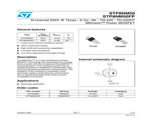
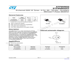
STP8NM50 STP8NM50FP N-channel 550V @ Tjmax - 0.7 - 8A - TO-220 - TO-220FP MDmeshTM Power MOSFET General features Type VDSS (@Tjmax) RDS(on) STP8NM50 550V <0.8 8A STP8NM50FP 550V <0.8 8A (1) ID 1. Limited only by maximum temperature allowed 3 1 100% avalanche tested High dv/dt and avalanche capabilities Low gate input resistance Low input capacitance and gate charge TO-220 3 2 1 2 TO-220FP Description The MDmeshTM is a new revolutionary Power MOSFET technology that associates the multiple drain process with the company's PowerMESHTM horizontal layout. The resulting product has an outstanding low on-resistance, impressively high dv/dt and excellent avalanche characteristics. The adoption of the company's proprietary strip technique yields overall dynamic performance that is significantly better than that of similar competition's products. Internal schematic diagram Applications Switching application Order codes Part number Marking Package Packaging STP8N
 14 Pages, 258 KB, Original
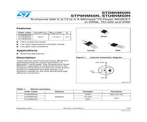
STP8NM50N Datasheet N-channel 500 V, 0.73 typ., 5 A, MDmeshTM II Power MOSFETs in DPAK and TO-220 packages Features Order codes TAB TAB VDS @ TJmax RDS(on) max. ID 550 V 0.79 5A STD8NM50N 2 3 1 STP8NM50N TO-220 DPAK 1 2 3 * * * 100% avalanche tested Low input capacitance and gate charge Low gate input resistance Applications D(2, TAB) * Switching applications Description G(1) S(3) AM01475v1_noZen These devices are N-channel Power MOSFETs developed using the second generation of MDmeshTM technology. These revolutionary Power MOSFETs associate a vertical structure to the company's strip layout to yield one of the world's lowest on-resistance and gate charge. They are therefore suitable for the most demanding high-efficiency converters. Product status links STD8NM50N STP8NM50N Product summary Order code STD8NM50N Marking 8NM50N Package DPAK Packing Tape and reel Order code STP8NM50N Marking 8NM50N Package TO-220 Packing Tube DS6808 - Rev 7 - September 2018 For
 21 Pages, 664 KB, Original
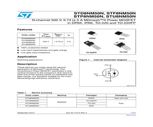
STP8NM50N, STU8NM50N N-channel 500 V, 0.73 typ., 5 A MDmeshTMII Power MOSFET in DPAK, TO-220 and IPAK packages Datasheet -- production data Features TAB Order codes VDSS@TJMAX RDS(on)max. STD8NM50N STP8NM50N STU8NM50N ID 3 1 550 V < 0.79 DPAK 5A TAB 100% avalanche tested Low input capacitance and gate charge Low gate input resistance TAB 1 Applications 3 3 2 2 1 IPAK TO-220 Switching applications Description Figure 1. These devices are N-channel Power MOSFETs developed using the second generation of MDmeshTM technology. This revolutionary Power MOSFET associates a vertical structure to the company's strip layout to yield one of the world's lowest on-resistance and gate charge. It is therefore suitable for the most demanding high efficiency converters. Internal schematic diagram $ 4!" ' 3 !-V Table 1. Device summary Order codes Marking Packages Packaging DPAK Tape and reel STD8NM50N STP8NM50N 8NM50N TO-220 Tube STU8NM50N September 2012 This is information on a product in
 19 Pages, 1160 KB, Original
STP8NM50 STP8NM50FP N-channel 550V @ Tjmax - 0.7 - 8A - TO-220 - TO-220FP MDmeshTM Power MOSFET General features Type VDSS (@Tjmax) RDS(on) STP8NM50 550V <0.8 8A STP8NM50FP 550V <0.8 8A (1) ID 1. Limited only by maximum temperature allowed 100% avalanche tested High dv/dt and avalanche capabilities Low gate input resistance Low input capacitance and gate charge 2 TO-220 e t e ol Description The MDmeshTM is a new revolutionary Power MOSFET technology that associates the multiple drain process with the company's PowerMESHTM horizontal layout. The resulting product has an outstanding low on-resistance, impressively high dv/dt and excellent avalanche characteristics. The adoption of the company's proprietary strip technique yields overall dynamic performance that is significantly better than that of similar competition's products. du 3 1 ) s ( ct ) (s o r P 3 1 2 TO-220FP s b O Internal schematic diagram t c u d o r P e t e l Applications o s b OOrder codes Swit
 14 Pages, 290 KB, Original
. . . . . . . . . . . . . . . . . . . . . . . . . . . . . . . . . . . . . . . 16 Capacitive losses . . . . . . . . . . . . . . . . . . . . . . . . . . . . . . . . . . . . . . . . . . . . . . . . . . . . . . . . 16 Conduction losses and total losses in the STP8NM50 MOSFET for the 80W TM PFC . . . 17 L6562A internal schematic . . . . . . . . . . . . . . . . . . . . . . . . . . . . . . . . . . . . . . . . . . . . . . . . . 18 Bode plot - open-loop transfer function. . . . . . . . . . . . . . . . . . . . . . . . . . . . . . . . . . . . . . . . 20 Bode plot - phase . . . . . . . . . . . . . . . . . . . . . . . . . . . . . . . . . . . . . . . . . . . . . . . . . . . . . . . . 20 Multiplier characteristics family . . . . . . . . . . . . . . . . . . . . . . . . . . . . . . . . . . . . . . . . . . . . . . 22 Optimum MOSFET turn-on . . . . . . . . . . . . . . . . . . . . . . . . . . . . . . . . . . . . . . . . . . . . . . . . . 24 Excel spreadsheet design specification input table . . . . . . . . . . . . .
 36 Pages, 564 KB, Original
STP8NM50 STP8NM50FP N-channel 550V @ Tjmax - 0.7 - 8A - TO-220 - TO-220FP MDmeshTM Power MOSFET General features Type VDSS (@Tjmax) RDS(on) STP8NM50 550V <0.8 8A STP8NM50FP 550V <0.8 8A (1) ID 1. Limited only by maximum temperature allowed 3 1 100% avalanche tested High dv/dt and avalanche capabilities Low gate input resistance Low input capacitance and gate charge TO-220 3 2 1 2 TO-220FP Description The MDmeshTM is a new revolutionary Power MOSFET technology that associates the multiple drain process with the company's PowerMESHTM horizontal layout. The resulting product has an outstanding low on-resistance, impressively high dv/dt and excellent avalanche characteristics. The adoption of the company's proprietary strip technique yields overall dynamic performance that is significantly better than that of similar competition's products. Internal schematic diagram Applications Switching application Order codes Part number Marking Package Packaging STP8N
 14 Pages, 273 KB, Original
STP8NM50N, STU8NM50N N-channel 500 V, 0.73 , 5 A MDmeshTMII Power MOSFET in DPAK, IPAK, TO-220 and TO-220FP Features Order codes VDSS @TJMAX STD8NM50N STF8NM50N STP8NM50N STU8NM50N RDS(on) max. 3 ID 3 1 2 1 DPAK 550 V < 0.79 IPAK 5A 100% avalanche tested Low input capacitances and gate charge Low gate input resistance 3 1 3 2 1 2 TO-220 TO-220FP Application Figure 1. Switching applications Internal schematic diagram Description $ These devices are made using the second generation of MDmeshTM technology. This revolutionary Power MOSFET associates a new vertical structure to the company's strip layout to yield one of the world's lowest on-resistance and gate charge. It is therefore suitable for the most demanding high efficiency converters. ' 3 !-V Table 1. Device summary Order codes Marking Packages Packaging DPAK Tape and reel STD8NM50N STF8NM50N TO-220FP 8NM50N STP8NM50N TO-220 STU8NM50N IPAK September 2010 Doc ID 17413 Rev 2 Tube 1/17 www.st.com 17 Contents STD8NM50N,
 17 Pages, 525 KB, Original
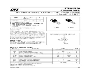
STP8NM50 STP8NM50FP N-CHANNEL 550V @ Tjmax 0.7 - 8A TO-220/TO-220FP MDmeshTM MOSFET TYPE STP8NM50 STP8NM50FP VDSS (@Tjmax) RDS(on) ID 550V 550V < 0.8 < 0.8 8A 8A TYPICAL RDS(on) = 0.7 HIGH dv/dt AND AVALANCHE CAPABILITIES 100% AVALANCHE TESTED LOW INPUT CAPACITANCE AND GATE CHARGE LOW GATE INPUT RESISTANCE DESCRIPTION The MDmeshTM is a new revolutionary MOSFET technology that associates the Multiple Drain process with the Company's PowerMESHTM horizontal layout. The resulting product has an outstanding low on-resistance, impressively high dv/dt and excellent avalanche characteristics. The adoption of the Company's proprietary strip technique yields overall dynamic performance that is significantly better than that of similar competition's products. 3 3 1 2 1 TO-220 2 TO-220FP INTERNAL SCHEMATIC DIAGRAM APPLICATIONS The MDmeshTM family is very suitable for increasing power density of high voltage converters allowing system miniaturization and higher efficienc
 9 Pages, 225 KB, Original
20N06 FQPF28N15 FQPF2N50 FQPF2N50C FQPF2N60 FQPF2N60C FQPF2N80 FQPF2N90 FQPF2NA90 FQPF30N06 FQPF32N12V2 FQPF32N20C 8 STP80NF10 STP40NF10 STP8NM60 STP9NK65Z STP8NK80Z STP7NK80Z STP6NK60Z STP8NK80Z STP6NK90Z STP80NF10 STP120NF10 STP8NS25 STP8NS25 STP12NK30Z STP8NM50 STP8NM50 STP9NK90Z IRF630FP IRF630FP STP10NK60ZFP STP11NK40ZFP STP11NK40ZFP STF12PF06 STP10NK60ZFP STP10NK60ZFP STP14NF12FP STP12NM50FDFP STP11NK50ZFP STP16NS25FP STP17NK40ZFP STF20N20 STF20NM50D STF20N20 IRF640FP STF20NF06L STP30NS15LFP STP4NK50ZFP STF2HNK60Z STF2HNK60Z STP3NK90ZFP STP36NF06FP Direct ST nearest Fairchild STP40NF10 STP80NF12 STP14NF12 IRF630 STP7NK30Z STP7NK40Z STP6NK60Z STP5NK65Z STP7NK80Z STP5NK80Z STP80NF06 STP8NS25 STP5NK60Z STP7NK80Z STP9NK90Z STP40NF10 STP80NF10 STP14NF10 STP16NS25 STP16NS25 STP11NK50Z STP9NK50Z STP6NK90Z STP13NK60ZFP STP17NK40ZFP IRF640FP STP13NK60ZFP STP13NK60ZFP STP16NF06FP STP11NK50ZFP STP12NM50FDFP STP30NS15LFP STP16NS25FP STF12PF06 IRF640FP STP15NK50ZFP STF24NF12 IRF640FP STF20N
 36 Pages, 584 KB, Original
STP8NM50 STP8NM50FP N-CHANNEL 500V - 0.7 - 8A TO-220/TO-220FP MDmesh Power MOSFET TYPE STP8NM50 STP8NM50FP VDSS RDS(on) ID 500V 500V < 0.8 < 0.8 8A 8A TYPICAL RDS(on) = 0.7 HIGH dv/dt AND AVALANCHE CAPABILITIES 100% AVALANCHE TESTED LOW INPUT CAPACITANCE AND GATE CHARGE LOW GATE INPUT RESISTANCE DESCRIPTION The MDmesh is a new revolutionary MOSFET technology that associates the Multiple Drain process with the Company's PowerMESH horizontal layout. The resulting product has an outstanding low on-resistance, impressively high dv/dt and excellent avalanche characteristics. The adoption of the Company's proprietary strip technique yields overall dynamic performance that is significantly better than that of similar competition's products. 3 3 1 2 1 TO-220 2 TO-220FP INTERNAL SCHEMATIC DIAGRAM APPLICATIONS The MDmesh family is very suitable for increasing power density of high voltage converters allowing system miniaturization and higher efficiencies. ABSOLUTE MAX
 9 Pages, 102 KB, Original
STP8NM50N, STU8NM50N N-channel 500 V, 0.73 typ., 5 A MDmeshTMII Power MOSFET in DPAK, TO-220 and IPAK packages Datasheet -- production data Features TAB Order codes VDSS@TJMAX RDS(on)max. STD8NM50N STP8NM50N STU8NM50N ID 3 1 550 V < 0.79 DPAK 5A TAB 100% avalanche tested Low input capacitance and gate charge Low gate input resistance TAB 1 Applications 3 3 2 2 1 IPAK TO-220 Switching applications Description Figure 1. These devices are N-channel Power MOSFETs developed using the second generation of MDmeshTM technology. This revolutionary Power MOSFET associates a vertical structure to the company's strip layout to yield one of the world's lowest on-resistance and gate charge. It is therefore suitable for the most demanding high efficiency converters. Internal schematic diagram $ 4!" ' 3 !-V Table 1. Device summary Order codes Marking Packages Packaging DPAK Tape and reel STD8NM50N STP8NM50N 8NM50N TO-220 Tube STU8NM50N September 2012 This is information on a product in
 20 Pages, 1146 KB, Original
STP8NM50N, STU8NM50N N-channel 500 V, 0.73 , 5 A MDmeshTMII Power MOSFET in DPAK, TO-220 and IPAK Features TAB Order codes VDSS@TJMAX RDS(on)max. STD8NM50N STP8NM50N STU8NM50N ID 3 1 550 V < 0.79 DPAK 5A TAB 100% avalanche tested Low input capacitances and gate charge Low gate input resistance TAB 1 Applications 3 3 2 2 1 IPAK TO-220 Switching applications Description Figure 1. These devices are N-channel Power MOSFETs developed using the second generation of MDmeshTM technology. This revolutionary Power MOSFET associates a vertical structure to the company's strip layout to yield one of the world's lowest on-resistance and gate charge. It is therefore suitable for the most demanding high efficiency converters. Internal schematic diagram $ 4!" ' 3 !-V Table 1. Device summary Order codes Marking Packages Packaging DPAK Tape and reel STD8NM50N STP8NM50N 8NM50N TO-220 Tube STU8NM50N November 2011 IPAK Doc ID 17413 Rev 5 1/19 www.st.com 19 Contents STD8NM50N, STP8NM50<
 19 Pages, 529 KB, Original
STP8NM50 STP8NM50FP N-CHANNEL 500V - 0.7 - 8A TO-220/TO-220FP MDmeshTMPower MOSFET TYPE STP8NM50 STP8NM50FP n n n n n VDSS RDS(on) ID 500V 500V < 0.8 < 0.8 8A 8A TYPICAL RDS(on) = 0.7 HIGH dv/dt AND AVALANCHE CAPABILITIES 100% AVALANCHE TESTED LOW INPUT CAPACITANCE AND GATE CHARGE LOW GATE INPUT RESISTANCE DESCRIPTION The MDmeshTM is a new revolutionary MOSFET technology that associates the Multiple Drain process with the Company's PowerMESHTM horizontal layout. The resulting product has an outstanding low on-resistance, impressively high dv/dt and excellent avalanche characteristics. The adoption of the Company's proprietary strip technique yields overall dynamic performance that is significantly better than that of similar competition's products. 3 3 1 2 1 TO-220 2 TO-220FP INTERNAL SCHEMATIC DIAGRAM APPLICATIONS The MDmeshTM family is very suitable for increasing power density of high voltage converters allowing system miniaturization and higher efficienc
 9 Pages, 220 KB, Original
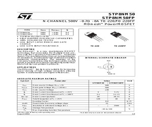
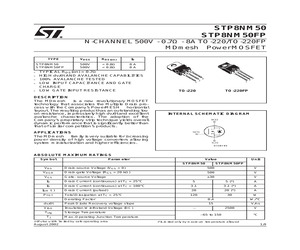
STP8NM50 STP8NM50FP N-CHANNEL 500V - 0.7 - 8A TO-220/TO-220FP MDmesh Power MOSFET TYPE STP8NM50 STP8NM50FP n n n n n VDSS RDS(on) ID 500V 500V < 0.8 < 0.8 8A 8A TYPICAL RDS(on) = 0.7 HIGH dv/dt AND AVALANCHE CAPABILITIES 100% AVALANCHE TESTED LOW INPUT CAPACITANCE AND GATE CHARGE LOW GATE INPUT RESISTANCE DESCRIPTION The MDmesh is a new revolutionary MOSFET technology that associates the Multiple Drain process with the Company's PowerMESH horizontal layout. The resulting product has an outstanding low on-resistance, impressively high dv/dt and excellent avalanche characteristics. The adoption of the Company's proprietary strip technique yields overall dynamic performance that is significantly better than that of similar competition's products. 3 3 1 2 1 TO-220 2 TO-220FP INTERNAL SCHEMATIC DIAGRAM APPLICATIONS The MDmesh family is very suitable for increasing power density of high voltage converters allowing system miniaturization and higher efficiencies. AB
 9 Pages, 103 KB, Original
STP8NM50 STP8NM50FP N-CHANNEL 500V - 0.7 - 8A TO-220/TO-220FP MDmesh Power MOSFET TYPE STP8NM50 STP8NM50FP VDSS RDS(on) ID 500V 500V < 0.8 < 0.8 8A 8A TYPICAL RDS(on) = 0.7 HIGH dv/dt AND AVALANCHE CAPABILITIES 100% AVALANCHE TESTED LOW INPUT CAPACITANCE AND GATE CHARGE LOW GATE INPUT RESISTANCE DESCRIPTION The MDmesh is a new revolutionary MOSFET technology that associates the Multiple Drain process with the Company's PowerMESH horizontal layout. The resulting product has an outstanding low on-resistance, impressively high dv/dt and excellent avalanche characteristics. The adoption of the Company's proprietary strip technique yields overall dynamic performance that is significantly better than that of similar competition's products. 3 3 1 2 1 TO-220 2 TO-220FP INTERNAL SCHEMATIC DIAGRAM APPLICATIONS The MDmesh family is very suitable for increasing power density of high voltage converters allowing system miniaturization and higher efficiencies. ABSOLUTE MAX
 9 Pages, 102 KB, Original


