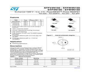
STW4N150 N-channel 1500 V - 5 - 4 A - PowerMESHTM Power MOSFET TO-220 - TO-220FH - TO-247 - TO-3PF Features Type VDSS RDS(on) max ID STFV4N150 STFW4N150 (1) STP4N150 STW4N150 1500 V 1500 V 1500 V 1500 V <7 <7 <7 <7 4A 4A 4A 4A 3 1 2 2 TO-220 3 1 TO-247 1. All data which refers solely to the TO-3PF package is preliminary 3 100% avalanche tested Intrinsic capacitances and Qg minimized High speed switching Fully isolated TO-3PF and TO-220FH plastic packages Creepage distance path is 5.4 mm (typ.) for TO-3PF Creepage distance path is > 4 mm for TO-220FH 1 TO-3PF Figure 1. 2 2 1 3 TO-220FH Internal schematic diagram. Application Switching applications Description Using the well consolidated high voltage MESH OVERLAYTM process, STMicroelectronics has designed an advanced family of very high voltage Power MOSFETs with outstanding performances. The strengthened layout coupled with the company's proprietary edge termination structure, gives the lowest RDS(on) per area, unrivalled gate charge
 16 Pages, 358 KB, Original
STW4N150 N-channel 1500 V, 5 , 4 A, PowerMESHTM Power MOSFET in TO-220, TO-247, TO-3PF Features Type VDSS RDS(on) max ID Pw STFW4N150 1500 V <7 4A 63 W STP4N150 1500 V <7 4A 160 W STW4N150 1500 V <7 4A 160 W 2 2 3 1 TO-220 TO-247 100% avalanche tested Intrinsic capacitances and Qg minimized High speed switching Fully isolated TO-3PF plastic packages Creepage distance path is 5.4 mm (typ.) for TO-3PF 3 1 2 TO-3PF Application 3 1 Figure 1. Internal schematic diagram. Switching applications $ Description Using the well consolidated high voltage MESH OVERLAYTM process, STMicroelectronics has designed an advanced family of very high voltage Power MOSFETs with outstanding performances. The strengthened layout coupled with the company's proprietary edge termination structure, gives the lowest RDS(on) per area, unrivalled gate charge and switching characteristics. ' 3 !-V Table 1. Device summary Order codes Marking Package Packaging STFW4N150 4N150 TO-3PF Tube STP4N150 P4N150 TO-220 Tube 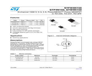 15 Pages, 758 KB, Original
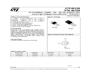
15 Pages, 758 KB, OriginalSTW4N150 N-CHANNEL 1500V - 5 - 4A TO-220/TO-247 Very High Voltage PowerMESHTM MOSFET Figure 1: Package Table 1: General Features TYPE STP4N150 STW4N150 VDSS RDS(on) ID Pw 1500 V 1500 V <7 <7 4A 4A 160 W 160 W TYPICAL RDS(on) = 5 AVALANCHE RUGGEDNESS GATE CHARGE MINIMIZED VERY LOW INTRINSIC CAPACITANCES HIGH SPEED SWITCHING 3 1 3 2 2 1 TO-220 DESCRIPTION Using the well consolidated high voltage MESH OVERLAYTM process, STMicroelectronics has designed an advanced family of Power MOSFETs with outstanding performances. The strengthened layout coupled with the Company's proprietary edge termination structure, gives the lowest RDS(on) per area, unrivalled gate charge and switching characteristics. TO-247 Figure 2: Internal Schematic Diagram APPLICATIONS SWITCH MODE POWER SUPPLIES Table 2: Order Codes SALES TYPE MARKING PACKAGE PACKAGING STP4N150 P4N150 TO-220 TUBE STW4N150 W4N150 TO-247 TUBE Rev. 3 July 2005 1/11 STP4N150 - STW4N150 Table 3: Absolute Maximum rating
 11 Pages, 252 KB, Original
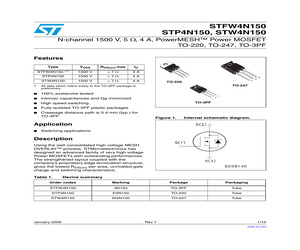
STW4N150 N-channel 1500 V, 5 , 4 A, PowerMESHTM Power MOSFET in TO-220, TO-247, TO-3PF Features Type VDSS RDS(on) max ID Pw STFW4N150 1500 V <7 4A 63 W STP4N150 1500 V <7 4A 160 W STW4N150 1500 V <7 4A 160 W 2 2 3 1 TO-220 TO-247 100% avalanche tested Intrinsic capacitances and Qg minimized High speed switching Fully isolated TO-3PF plastic packages Creepage distance path is 5.4 mm (typ.) for TO-3PF 3 1 2 TO-3PF Application 3 1 Figure 1. Internal schematic diagram. Switching applications $ Description Using the well consolidated high voltage MESH OVERLAYTM process, STMicroelectronics has designed an advanced family of very high voltage Power MOSFETs with outstanding performances. The strengthened layout coupled with the company's proprietary edge termination structure, gives the lowest RDS(on) per area, unrivalled gate charge and switching characteristics. ' 3 !-V Table 1. Device summary Order codes Marking Package Packaging STFW4N150 4N150 TO-3PF Tube STP4N150 P4N150 TO-220 Tube  16 Pages, 741 KB, Original
16 Pages, 741 KB, OriginalSTW4N150 N-channel 1500 V, 5 , 4 A, PowerMESHTM Power MOSFET TO-220, TO-247, TO-3PF Features Type VDSS RDS(on) max ID 1500 V <7 4A STP4N150 1500 V <7 4A STW4N150 1500 V <7 4A STFW4N150 (1) 3 1 2 2 TO-220 TO-247 1. All data which refers solely to the TO-3PF package is preliminary 100% avalanche tested Intrinsic capacitances and Qg minimized High speed switching Fully isolated TO-3PF plastic packages Creepage distance path is 5.4 mm (typ.) for TO-3PF 3 1 3 1 2 TO-3PF Figure 1. Internal schematic diagram. Application Switching applications Description Using the well consolidated high voltage MESH OVERLAYTM process, STMicroelectronics has designed an advanced family of very high voltage Power MOSFETs with outstanding performances. The strengthened layout coupled with the company's proprietary edge termination structure, gives the lowest RDS(on) per area, unrivalled gate charge and switching characteristics. Table 1. Device summary Order codes Marking Package Packaging STFW4N150 4N150 TO-
 15 Pages, 387 KB, Original
STW4N150 N-channel 1500 V, 5 , 4 A, PowerMESHTM Power MOSFET TO-220, TO-247, TO-3PF Features Type VDSS RDS(on) max ID 1500 V <7 4A STP4N150 1500 V <7 4A STW4N150 1500 V <7 4A STFW4N150 (1) 3 1 2 2 TO-220 TO-247 1. All data which refers solely to the TO-3PF package is preliminary 100% avalanche tested Intrinsic capacitances and Qg minimized High speed switching Fully isolated TO-3PF plastic packages Creepage distance path is 5.4 mm (typ.) for TO-3PF 3 1 3 1 2 TO-3PF Figure 1. Internal schematic diagram. Application Switching applications Description Using the well consolidated high voltage MESH OVERLAYTM process, STMicroelectronics has designed an advanced family of very high voltage Power MOSFETs with outstanding performances. The strengthened layout coupled with the company's proprietary edge termination structure, gives the lowest RDS(on) per area, unrivalled gate charge and switching characteristics. Table 1. Device summary Order codes Marking Package Packaging STFW4N150 4N150 TO-
 15 Pages, 364 KB, Original
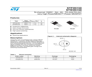
STW4N150 N-channel 1500V - 5 - 4A - TO-220/TO-247 very high PowerMESHTM Power MOSFET Features VDSS RDS(on) Max (@Tjmax) Type ID STP4N150 1500 V <7 4A STW4N150 1500 V <7 4A Avalanche ruggedness Gate charge minimized Very low intrinsic capacitances High speed switching 3 1 TO-220 2 2 3 1 TO-247 Application Switching applications Figure 1. Internal schematic diagram Description Using the well consolidated high voltage MESH OVERLAYTM process, STMicroelectronics has designed an advanced family of Power MOSFETs with outstanding performances. The strengthened layout coupled with the Company's proprietary edge termination structure, gives the lowest RDS(on) per area, unrivalled gate charge and switching characteristics. Table 1. Device summary Order codes Marking Package Packaging STP4N150 P4N150 TO-220 Tube STW4N150 W4N150 TO-247 Tube November 2007 Rev 5 1/14 www.st.com 14 Contents STP4N150 - STW4N150 Contents 1 Electrical ratings . . . . . . . . . . . . . . . . .
 14 Pages, 298 KB, Original
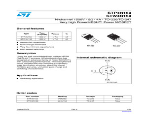
STW4N150 N-channel 1500V - 5 - 4A - TO-220/TO-247 Very high PowerMESHTM Power MOSFET General features Type VDSS (@Tjmax) RDS(on) ID STP4N150 1500 V <7 4A STW4N150 1500 V <7 4A Avalanche ruggedness Gate charge minimized Very low intrinsic capacitances High speed switching 3 1 TO-220 2 TO-247 Description Using the well consolidated high voltage MESH OVERLAYTM process, STMicroelectronics has designed an advanced family of Power MOSFETs with outstanding performances. The strengthened layout coupled with the Company's proprietary edge termination structure, gives the lowest RDS(on) per area, unrivalled gate charge and switching characteristics. Internal schematic diagram Applications Switching application Order codes Part number Marking Package Packaging STP4N150 P4N150 TO-220 Tube STW4N150 W4N150 TO-247 Tube August 2006 Rev 4 1/14 www.st.com 14 Contents STP4N150 - STW4N150 Contents 1 Electrical ratings . . . . . . . . . . . . . . . . . . . . . . . . . . . . . .
 14 Pages, 340 KB, Original
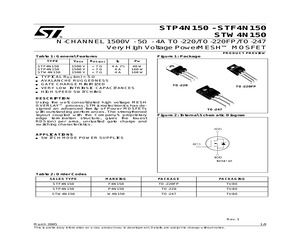
STW4N150 N-CHANNEL 1500V - 5 - 4A TO-220/TO-247 Very High Voltage PowerMESHTM MOSFET PRODUCT PREVIEW Figure 1: Package Table 1: General Features TYPE STP4N150 STW4N150 VDSS RDS(on) ID Pw 1500 V 1500 V <7 <7 4A 4A 160 W 160 W TYPICAL RDS(on) = 5 AVALANCHE RUGGEDNESS GATE CHARGE MINIMIZED VERY LOW INTRINSIC CAPACITANCES HIGH SPEED SWITCHING 3 1 3 2 2 1 TO-220 DESCRIPTION Using the well consolidated high voltage MESH OVERLAYTM process, STMicroelectronics has designed an advanced family of Power MOSFETs with outstanding performances. The strengthened layout coupled with the Company's proprietary edge termination structure, gives the lowest RDS(on) per area, unrivalled gate charge and switching characteristics. TO-247 Figure 2: Internal Schematic Diagram APPLICATIONS SWITCH MODE POWER SUPPLIES Table 2: Order Codes SALES TYPE MARKING PACKAGE PACKAGING STP4N150 P4N150 TO-220 TUBE STW4N150 W4N150 TO-247 TUBE Rev. 2 April 2005 This is preliminary information on a new product now
 8 Pages, 103 KB, Original
STW4N150 N-CHANNEL 1500V - 5 - 4A TO-220/TO-220FP/TO-247 Very High Voltage PowerMESHTM MOSFET PRODUCT PREVIEW Figure 1: Package Table 1: General Features TYPE STF4N150 STP4N150 STW4N150 VDSS RDS(on) ID Pw 1500 V 1500 V 1500 V <7 <7 <7 4 A (*) 4A 4A 40 W 160 W 160 W TYPICAL RDS(on) = 5 AVALANCHE RUGGEDNESS GATE CHARGE MINIMIZED VERY LOW INTRINSIC CAPACITANCES HIGH SPEED SWITCHING DESCRIPTION Using the well consolidated high voltage MESH OVERLAYTM process, STMicroelectronics has designed an advanced family of Power MOSFETs with outstanding performances. The strengthened layout coupled with the Company's proprietary edge termination structure, gives the lowest RDS(on) per area, unrivalled gate charge and switching characteristics. 3 1 2 3 1 TO-220 2 TO-220FP 3 2 1 TO-247 Figure 2: Internal Schematic Diagram APPLICATIONS SWITCH MODE POWER SUPPLIES Table 2: Order Codes SALES TYPE MARKING PACKAGE PACKAGING STF4N150 F4N150 TO-220FP TUBE STP4N150 P4N150 TO-220 TUBE STW4N150 W4N1
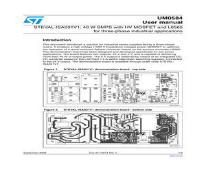
 9 Pages, 129 KB, Original
 . . . . . . . . . . . . . . . . . . . . . . . . . . . . . 8 Doc ID 14974 Rev 1 UM0584 1 Demonstration board description Demonstration board description The STEVAL-ISA031V1 demonstration board is based on a quasi resonant flyback converter and employs the STW4N150 power MOSFET as the primary switch. The STW4N150 is a 5 1500 V power MOSFET designed with STMicroelectronics' proprietary high voltage "Mesh Overlay" technology, which gives the switch very low RDS(on) per area, low gate charge and high switching performance. The STW4N150 device is available in the TO-220, TO-247 and TO-220FH packages. The main specifications of the demonstration board are provided in table below. Table 1. STEVAL-ISA031V1 main specifications Parameter Value Input voltage range 185 to 460 Vac Input frequency range 50/60 Hz Output 1 24 V @ 1.7 A Output 2 5V@1A Output power 40 W Safety EN60950 EMI EN55014 The input section features two connectors: CON1 for 400 Vac input voltage and CON2 for 230 Va
 9 Pages, 386 KB, Original
witching losses. This key difference will value 1700V SiC MOSFET to have high efficiency and high reliability replacing 1500V Si MOSFET. Table 1: Parameter comparisons of 1700V SiC MOSFET and 1500V Si MOSFET Parameters SiC MOSFET Si MOS Si MOS C2M1000170D STW4N150 2SK2225DS V(BR)DSS 1700V 1500V 1500V Avalanche >1800V N/A N/A Id @ Tc=25C 5A 4A 2A Rdson @150C 2ohm 9ohm 20ohm Coss 14pF 120pF 60pF Tjmax >150C 150C 150C Package TO-247 TO-220, TO-247 TO-3PF 4. ACTIVE START-UP CIRCUIT In this design, a non-dissipative, active start-up circuit has been implemented to optimize converter efficiency and fast start-up time. The alternative is to use a pure resistive start-up circuit which significantly affects converter efficiency and start up times at low input voltages in a negative way. Figure 2 shows the proposed active start-up circuit. When input voltage is increasing, Q6 is turned on by Vbase from path R31 to R36. The VCC voltage comes from path R22 to R25 when U1 (UCC28C44) is turning on. Once U1 sta
 10 Pages, 1898 KB, Original
or Design Engineers - www.element-14.com VDS V 800 Polarity N ID cont RDS(on) @ 25C A 4.5 2.5 PD @ 25C W 25 Mftr. Package ST TO-220FP Order Code 129-1972 Mftrs. List No. STF3NK80Z 900 N 0.17 40 600 ST ISOTOP 129-1966 STE40NK90ZD 7 4 160 ST TO-247 125-2936 STW4N150 1500 N TO-220, N Channel 600V to 1500V VDS V 600 600 600 600 600 600 600 600 600 600 600 600 RDS(on) 0.55 0.75 0.75 1.2 1.2 1.2 1.2 1.2 2 2.2 3.6 3.6 ID cont @ 25C A 13 10 9.2 6 6 6.2 6.2 6.2 4 3.6 2.4 2.4 ID pulsed A 52 36 37 24 24 25 25 25 16 14 9.6 9.6 PD @ 25C W 150 115 170 110 110 125 125 125 70 74 45 45 Mftr. ST ST VISH ST ST VISH VISH VISH ST VISH ST ST Mftrs. List No. STP13NK60Z STP10NK60Z IRFB9N60APBF STP6NK60Z STP6NK60Z IRFBC40APBF IRFBC40PBF IRFBC40LCPBF STP4NK60Z IRFBC30APBF STP3NK60Z STP3NK60Z 800 800 800 800 1.8 2.4 3 8 5.2 4.3 4.1 1.5 20.8 17.2 16 6 125 110 125 40 ST ST VISH INF STP7NK80Z STP5NK80Z IRFBE30PBF SPP02N80C3 900 900 900 2 4.8 8 5.8 3 1.7 23.2 12 3.1 140 90 54 ST ST VISH STP6NK90Z STP3NK90Z IRFBF20PBF 1000 1000
 144 Pages, 26045 KB, Original
B5NK50ZT4 STP2NK90Z STP4NK60Z STP5NK60ZFP STW14NK60Z STW20NK50Z STW29NK50ZD STW26NM50 STW29NK50ZD STP9NK50ZFP STF2HNK60Z STW14NK60Z ST nearest STB16PF06LT4 STB16PF06LT4 STD3NK50ZT4 STP4NK50Z STP6NK50Z STP9NK50Z STW14NM50FD STW14NK50Z STW15NK50Z STP22NE10L STW4N150 STW14NM50FD STP3NK90Z STW7NK90Z STW9NK90Z STP7NK30Z STP3NK60Z STP5NK65Z STW10NK60Z STP6NK60ZFP STW13NK60Z STW15NK50Z STW20NM50FD STW45NM50 STW20NM50FD STF6NK50Z STF2NK60Z STW13NK60Z BSC052N03S BSC059N03S BSC079N03SG BSC094N03SG BSC119N03SG BSO052N03S BSO064N03S BSO072N03S BSO080P03S BSO094N03S BSO104N03S BSO119N03S BSO130P03S BSO150N03S BSO200N03S BSO200P03S BSO203SP BSO207P BSO211P BSO220N BSO301SL BSO301SP BSO303SP BSO350N03 BSO4410 STP3HNK90Z STF3HNK90Z STP5NK60Z STW4N150 STW26NM50 STP4NK50ZFP STD1NK60T4 STW9NK90Z STW11NK100Z IRF630FP STW10NK60Z STW20NM50FD STD1HNC60T4 STD17NF03LT4 STP4NK60ZFP STP5NK50ZFP STP9NK50ZFP STP5NK60ZFP STF2HNK60Z STP4NK50ZFP STW15NK50Z STB22NS25ZT4 STP3NK60ZFP STP8NS25 STP16NS25FP STP16NS25 STP
 36 Pages, 584 KB, Original
43N60DM2 511-STP43N60DM2 511-STP45N60DM2AG 511-STW43N60DM2 511-STW45N60DM2AG 511-STW50N65DM2AG 511-STW56N65DM2 511-STW58N65DM2AG 511-STW65N65DM2AG 511-STU2N80K5 511-STFU15N80K5 511-STF23N80K5 511-STW23N80K5 511-STW18NM80 511-STW65N80K5 511-STF12N120K5 511-STW4N150 511-STW12N150K5 511-STW9N150 511-STW21N150K5 511-STW3N170 STP34NM60N STW48N60DM2 STW56N60DM2 STW58N60DM2AG STW70N60DM2 STW72N60DM2AG STFI13N65M2 STFU13N65M2 STFU15NM65N STB34NM60ND STF28N60DM2 STP33N60DM2 STW33N60DM2 STFW38N65M5 STF43N60DM2 STP43N60DM2 STP45N60DM2AG STW43N60DM2 STW45N60DM2AG STW50N65DM2AG STW56N65DM2 STW58N65DM2AG STW65N65DM2AG STU2N80K5 STFU15N80K5 STF23N80K5 STW23N80K5 STW18NM80 STW65N80K5 STF12N120K5 STW4N150 STW12N150K5 STW9N150 STW21N150K5 STW3N170 For quantities greater than listed, call for quote. Package Drain Source Breakdown Voltage (Min.) (V) Drain Current (Max.) (A) Total Dissipation @ 25C (Max.) (W) TO-220AB TO-247-3 TO-247-3 TO-247-3 TO-247-3 TO-247-3 I2PAK-3 TO-220FP-3 TO-220FP-3 D2PAK TO-220
 1 Pages, 227 KB, Original


