2SD72 2SB407 2N442 2N2482 2SD186 2SB337 2N174A 2SA603 2N3799 2N1306 2SB324 2SD352 2N2077 2N3251 ECG107 ECG108 ECG109 ECG110M ECG112 1SS99 ECG113A ECG114 ECG115 ECG116 ECG117 ECG118 ECG119 ECG121 ECG123 ECG123A ECG123AP ECG124 2SD24Y ECG125 1N5054 2SC1215 2N5770 1N60 1N542 1S750 2SC784 JE9016 1S188FM 1S188F 1S1922 DS-17 DS-19 DS-18 1N4007 1S1694 HVT-30S HVT-185 2SB471 2N1420 2N2222A 2N4401 2SC515A 2SC1059 1N5399 V03J DS-131 DS-133 DS-132 1N3549 1N5412 US144HFP US17HFP 2SB375 2N1711 ECG126A ECG127 2N3731 ECG128 ECG128P ECG129 ECG129P ECG130 2SD492 ECG131 ECG132 ECG133 ECG134A ECG135A ECG136A ECG137A ECG138A ECG139A ECG140A ECG141A ECG142A ECG143A ECG144A ECG145A ECG146A ECG147A ECG148A ECG149A ECG150A ECG151A ECG152 2SC789 2N2258 2SB411TV 2N3053 2SC1384 2N4036 2SA684 2N3055 2N3716 AD162 A5T3823 2N3819 1N4729A 1N4733A 1N4734A 1N4735A 1N4737A 1N4739A 1N4740A 1N4741A 1N4742A 1N4743A 1N4701A 1N4744A 1N4750A 1N4752A 1N4758A 1N4759A 1N4762A 1N4187B 2SD235 2SC717 JE9018 1N34M 1SS16 1N2070 1N5399 2N457B 2
 314 Pages, 275 KB, Original
04,TO-92,EBC TR-NPN,KSC945,TO-92,EBC TR-NPN,2N3904,TO-92,EBC TR-NPN,KSC945,TO-92,EBC KSP2222A,NPN,625mW,TO-92,TP,10 MPS3646,NPN,625mW,TO-92,30-1 2N3906,PNP,625mW,TO-92,TP,1002N3906,PNP,625mW,TO-92,TP,1002N3906,PNP,625mW,TO-92,TP,100TR-NPN,KSC945,TO-92,EBC 2N5770,NPN,450mW,TO-92,TP 2N5770,NPN,450mW,TO-92,TP TR-NPN,MPSA42,TO-92,EBC TR-PNP,MPSA92,TO-92,EBC 2N5770,NPN,450mW,TO-92,TP 2N5770,NPN,450mW,TO-92,TP TR-NPN,MPSA42,TO-92,EBC TR-PNP,MPSA92,TO-92,EBC 2N5770,NPN,450mW,TO-92,TP 2N5770,NPN,450mW,TO-92,TP TR-NPN,MPSA42,TO-92,EBC 9-19 9 Electrical Parts List Loc. No. Coordinates (X,Y) QR105 R101 R102 R103 R104 R105 R106 R107 R108 R109 R110 R111 R112 R113 R114 R115 R116 R117 R118 R119 R120 R121 R122 R123 R124 R125 R126 R127 R128 R129 R130 R133 R134 R135 R136 R137 R138 R139 R140 R141 R142 R143 R144 R145 R146 R147 R148 9-20 175.9 49.5 49.5 46.3 50.5 50.5 46.3 97.9 89.7 95.3 100.6 109.1 109.1 101.1 101.1 100.2 146.1 108.2 100.9 98.1 148.2 1
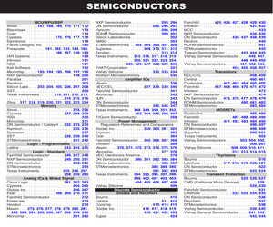
 90 Pages, 2115 KB, Original
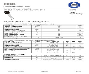
2N5770 TO-92 Plastic Package E BC VHF/UHF Amplifier Mixer and Oscillator Applications ABSOLUTE MAXIMUM RATINGS (Ta=25C unless specified otherwise) DESCRIPTION SYMBOL VCEO Collector Emitter Voltage VALUE 15 UNITS V Collector Base Voltage VCBO 30 V Emitter Base Voltage VEBO 4.5 V IC 50 mA PD 350 2.8 850 6.8 mW mW/ C mW mW/ C - 55 to +150 C Collector Current Continuous Power Dissipation@ Ta=25C Derate Above 25C Power Dissipation@ Tc=25C Derate Above 25C Operating And Storage Junction Temperature Range PD Tj, Tstg ELECTRICAL CHARACTERISTICS (Ta=25C unless specified otherwise) TEST CONDITION DESCRIPTION SYMBOL IC=3mA, IB=0 VCEO Collector Emitter Voltage MIN 15 MAX UNITS V Collector Base Voltage VCBO IC=10A, IE=0 30 V Emitter Base Voltage VEBO IE=10A, IC=0 VCB=15V, IE = 0 4.5 V ICBO 10 nA Collector Emitter Saturation Voltage VCE(sat) IC=10mA, IB=1mA 0.4 V Base Emitter Saturation Voltage VBE(sat) IC=10mA, IB=1mA 1.0 V Collector Cut Off Current DC Current Gain hFE DYNAMIC CHARACTERISTICS Output Capacitan
 3 Pages, 184 KB, Original
D44R2 2N3646 PN3646-18 2N3739 D42R2 2N3917 p44ce 2N3647 2N3013 2N3740 D45C7 2N3918 D44C8 2N3648 2N3013 2N3740A D457 2N3919 D4 208 2N3659 D44R1 2N3742 D40N3 2N3923 D44R1 2N3660 D4 303 2N3744 D44C5 2N3924 D4GOE1 2N3661 D43C8 2N3745 D44ce 2N3925 04201 2N3662 2N5770 2N3747 D44C6 2N3926 D40E 1 2N3663 2N5770 2N3748 D448 2N3927 D&401 2N3671 2N2905A 2N3762 D4 306 2N3932 2N5770 2N3672 2N2907A N3763 D43C8 2N3933 2N5770 2N3673 2N2907A 2N3766 D4408 2N3934 2N5196 2N3675 D4 207 2N3793 MPS6530 2N3935 2N5 196 2N3677 TP3677 2N3794 MPS6531 2N3945 D40E5 2N3678 D41E7 2N3798 2N3962 2N3948 D4OE1 2N 3680 2n2920 2N379B8A 2N3962 2N3953 2N5770 166
 1 Pages, 49 KB, Scan
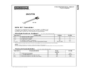
2N5770 C TO-92 BE NPN RF Transistor This device is designed for use as RF amplifiers, oscillators and multipliers with collector currents in the 1.0 mA to 30 mA range. Sourced from Process 43. See PN918 for characteristics. Absolute Maximum Ratings* Symbol TA = 25C unless otherwise noted Parameter Value Units V VCEO Collector-Emitter Voltage 15 VCBO Collector-Base Voltage 30 V VEBO Emitter-Base Voltage 4.5 V IC Collector Current - Continuous 50 mA TJ, Tstg Operating and Storage Junction Temperature Range -55 to +150 C *These ratings are limiting values above which the serviceability of any semiconductor device may be impaired. NOTES: 1) These ratings are based on a maximum junction temperature of 150 degrees C. 2) These are steady state limits. The factory should be consulted on applications involving pulsed or low duty cycle operations. Thermal Characteristics Symbol PD TA = 25C unless otherwise noted Characteristic RJC Total Device Dissipation Derate above 25C Thermal Resistance, Junction to Ca
 7 Pages, 278 KB, Original
2N5770 C TO-92 BE NPN RF Transistor This device is designed for use as RF amplifiers, oscillators and multipliers with collector currents in the 1.0 mA to 30 mA range. Sourced from Process 43. See PN918 for characteristics. Absolute Maximum Ratings* Symbol TA = 25C unless otherwise noted Parameter Value Units V VCEO Collector-Emitter Voltage 15 VCBO Collector-Base Voltage 30 V VEBO Emitter-Base Voltage 4.5 V IC Collector Current - Continuous 50 mA TJ, Tstg Operating and Storage Junction Temperature Range -55 to +150 C *These ratings are limiting values above which the serviceability of any semiconductor device may be impaired. NOTES: 1) These ratings are based on a maximum junction temperature of 150 degrees C. 2) These are steady state limits. The factory should be consulted on applications involving pulsed or low duty cycle operations. Thermal Characteristics Symbol PD TA = 25C unless otherwise noted Characteristic RJC Total Device Dissipation Derate above 25C Thermal Resistance, Junction to Ca
 2 Pages, 20 KB, Original
.6PI),-,-,AWG22(0. 52MM,AWG22(0.6PI),-,-,AWG22(0. 52MM,AWG22(0.6PI),-,-,AWG22(0. 52MM,AWG22(0.6PI),-,-,AWG22(0. 52MM,AWG22(0.6PI),-,-,AWG22(0. 52MM,AWG22(0.6PI),-,-,AWG22(0. 52MM,AWG22(0.6PI),-,-,AWG22(0. AQ19FS, FR1,115*80,1.0,1.6T,115*80*1.6T,AQUILA,-,-,2N5770,NPN,450mW,TO-92,TP,2N5770,NPN,450mW,TO-92,TP,2N5770,NPN,450mW,TO-92,TP,220OHM,5%,1/8W,AA,TP,1.8X3.2MM 52MM,AWG22(0.6PI),-,-,AWG22(0. 100OHM,5%,1/8W,AA,TP,1.8X3.2MM 15KOHM,5%,1/8W,AA,TP,1.8X3.2MM 33OHM,5%,1/8W,AA,TP,1.8X3.2MM 33OHM,5%,1/8W,AA,TP,1.8X3.2MM 100OHM,5%,1/8W,AA,TP,1.8X3.2MM 100OHM,5%,1/8W,AA,TP,1.8X3.2MM 100OHM,5%,1/8W,AA,TP,1.8X3.2MM 10KOHM,5%,1/8W,AA,TP,1.8X3.2MM 33OHM,5%,1/8W,AA,TP,1.8X3.2MM 75OHM,5%,1/8W,AA,TP,1.8X3.2MM 10OHM,5%,1/8W,AA,TP,1.8X3.2MM 75OHM,5%,1/8W,AA,TP,1.8X3.2MM 33OHM,5%,1/8W,AA,TP,1.8X3.2MM 22OHM,5%,1/8W,AA,TP,1.8X3.2MM 75OHM,5%,1/8W,AA,TP,1.8X3.2MM 10OHM,5%,1/8W,AA,TP,1.8X3.2MM SNA AQ17HS/AQ17IS/AQ17NS AQ19MS/AQ19IS/AQ19NS/AQ19FS 7 Electrical Parts List Loc. No. RG53 RG54 RG55 RR
 88 Pages, 2929 KB, Original
2N5770 TO-92 Plastic Package E BC VHF/UHF Amplifier Mixer and Oscillator Applications ABSOLUTE MAXIMUM RATINGS (Ta=25C unless specified otherwise) DESCRIPTION SYMBOL VCEO Collector Emitter Voltage VALUE 15 UNITS V Collector Base Voltage VCBO 30 V Emitter Base Voltage VEBO 4.5 V IC 50 mA PD 350 2.8 850 6.8 mW mW/ C mW mW/ C - 55 to +150 C Collector Current Continuous Power Dissipation@ Ta=25C Derate Above 25C Power Dissipation@ Tc=25C Derate Above 25C Operating And Storage Junction Temperature Range PD Tj, Tstg ELECTRICAL CHARACTERISTICS (Ta=25C unless specified otherwise) TEST CONDITION DESCRIPTION SYMBOL IC=3mA, IB=0 VCEO Collector Emitter Voltage MIN 15 MAX UNITS V Collector Base Voltage VCBO IC=10A, IE=0 30 V Emitter Base Voltage VEBO IE=10A, IC=0 VCB=15V, IE = 0 4.5 V ICBO 10 nA Collector Emitter Saturation Voltage VCE(sat) IC=10mA, IB=1mA 0.4 V Base Emitter Saturation Voltage VBE(sat) IC=10mA, IB=1mA 1.0 V Collector Cut Off Current DC Current Gain hFE DYNAMIC CHARACTERISTICS Output Capacitan
 3 Pages, 123 KB, Original
SA42 TO-92 40 - - - 50 .18 .105 .098 .091 610-2N3708 2N3708 TO-92 45 660 - - - .21 .168 .154 .14 610-2N2270 2N2270 TO-3950 200 100.92 .889 .855 .82 610-2N3903 2N3903 TO-9250 150 250.14 .127 .119 .112 610-2N4124 2N4124 TO-9250 200 300.06 .058 .054 .049 610-2N5770 2N5770 TO-9250 200 800.25 .224 .197 .175 610-2N4013 2N4013 TO-1860 150 300.92 .906 .889 .881 610-2N3725A 2N3725A TO-3960 150 300 1.34 1.28 1.21 1.18 .127 .112 610-2N2405 2N2405 TO-3960 200 50 .61 .589 .568 .554 610-2N4410 2N4410 TO-9260 400 60 .13 .119 .105 .098 610-MPSH10 MPSH10 TO-92 60 - - - 650 .25 .224 .197 .182 610-2N3416 2N3416 TO-92 75 225 - - - .13 .119 .105 .098 610-2N5551 2N5551 TO-9280 250 100.14 .127 .112 .098 610-2N2923 2N2923 TO-9290 180 160.27 .239 .21 610-MPS6531 MPS6531 TO-92 610-2N3107 2N3107 TO-39100 300 701.61 1.53 1.46 1.38 610-2N3501 2N3501 TO-39100 300 1503.64 3.57 3.45 3.36 90 270 - - - .20 .197 .119 .084 .077 610-2N3704 2N3704 TO-92100 300 100 .25 .232 .217 .203 610-2N5209 2N5209 TO-92100 300 30 .30
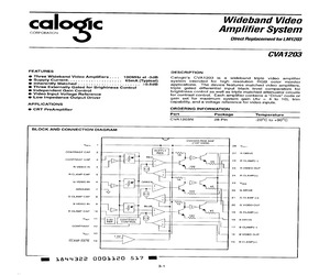
 379 Pages, 47721 KB, Original
10K CONTROL iL 10Ka tok@ | BLACK LEVEL MIN OtpF (BRIGHTNESS) Z Ww 10K | CONTROL __ O1pF 1R-46 BLACK LEVEL GATE IN vu c1 c2 c3 c4 | cLt } C6 | R4 {| RS R6 D1 D2 Li Qi pF uF LF pF pF pF Q K a2 nH CVA2415 1.0 0.01 0.1 0.47 12 1.0 34 1.5 150 FDH400 FDH400 560 2N5770 CVA2417 1.0 ; 0.01 01 [043] 12 1.0 | 34 | 1.5 | 150 | FDH400 FDH400 560 2N5770 CVA2419 1.0 1.0 0.1 | 0.47) 12 1.0 | 34 | 51 | 180 ; FDH400 FDH400 500 2N5770 MB 14443ee 0001123 ecb 3-4
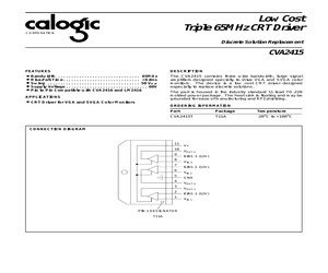
 4 Pages, 231 KB, Scan
 Vbias L1 3,4,10 Vout R5 VC C OUTPUT R4 CL D2 5 GND C1 = 0.01 F C2 = 0.01 F C3 = 0.1 F C4 = 0.47 F C L = 12pF (Including Parasitics) C6 = 1.0 F CALOGIC D1 C2 R1 = 8.2k R2 = 2.7k R3 = 10.0K R4 = 34 R5 = 1.5k R6 = 150 D1 = FDH400 D2 = FDH400 L1 = 560nH Q1 = 2N5770 CORPORATION, 237 Whitney Place, Fremont, California 94539, Telephone: 510-656-2900, FAX: 510-651-1076 CVA2415 CORPORATION APPLICATION INFORMATION FIGURE 2. CVA2415 DC Characteristics OUTPUT VOLTAGE (VOLTS) Thermal Considerations The transfer characteristics of the amplifier are shown in Figure 2. Since this is a class A input stage, power supply current increases as the input signal increases and consequently power dissipation also increases. Average dissipation per stage is 1.8W, increasing to 3.2W at minimum output voltage. The CVA2415 cannot be used without heat sinking. Figure 2 shows the power dissipated in each channel over the operating voltage range of the device, Typical "average" power dissipation with the device output voltage
 4 Pages, 41 KB, Original
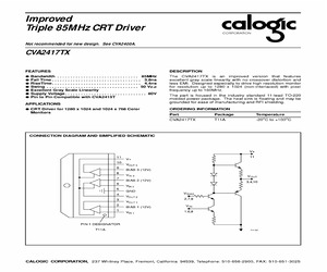
r Rise Time 44 6.0 ns tt Fall Time 3.8 5.0 ns BW Bandwidth 85 MHz Le Linearity 8 % Os Overshoot 10 % FIGURE 1. TEST CIRCUIT C1 = 0.01 nF R1 = 8.2kQ D1 = FDH400 C2 = 0.01 nF R2 = 2.7kQ D2 = FDH400 C3 = 0.1pF R3 = 10.0KQ L1 = 560nH C4 = 0.470F R4 = 340 Q1 = 2N5770 CL = 12pF (Including Parasitics) R5 = 1.5kQ C6 = 1.0NF R6 = 150Q 1H-33 CALOGIC CORPORATION, 237 Whitney Place, Fremont, California 94539, Telephone: 510-656-2900, FAX: 510-651-3025CVA2417TX APPLICATION INFORMATION The CVA2417TX is a high voltage triple CRT driver suitable for VGA, Super VGA, IBM 8514, 1280 x 1024 and 1024 x 768 non-interlaced display applications. The CVA2417TX features 80V operation and low power dissipation. The part is housed in the industry standard 11 lead TO-220 molded power package. The heat sink is floating and may be grounded for ease of manufacturing and RFI shielding. Thermal Considerations The transfer characteristics of the amplifier are shown in Figure 2. Since this is a class A input stage, power supply cur
 4 Pages, 110 KB, Scan
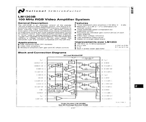
 or both. Note that an MM74C86 Exclusive-Or gate may also be used, however, the pin out is different than that of the MM74HC86. For optimum performance and maximum bandwidth, high speed buffer transistors (Q1, Q2, and Q3 in Figure 11) are recommended. The 2N5770 NPN transistors maintain high speed at high currents when driving the inputs of high volt- age CRT drivers. oe 1 28 - cree cps 0.01 uF ca Rod 100uF SS LM1203BN Re i 4 VY cr + 0.01 pF TOP VIEW ood oe R36 Ve og 3 26 30 SRI > RED ras 68 S200 R26 VIDEO 4 25 e rf 285770 IN 51 Our RZ R22 cB 390 10k R27 | 5 24 AAA VIDEO bay r R28 31 our GREEN pa 0? a ben ler gg S 23 oe oe we VIDEO H+ 5 'N 87 sour] @es RES SI rok (75) 7 bs Goiur BLUE rss C8 VIDEO } 9 IN 47 ron R? R62 51 4 tow o'9 (75) wo 10 R21 C19 te A 0.1 wt reed, 3 Wy R19 51 AY 390 R30 GREEN 9 AAAC) video N AA Vv or on oo el a7 =r nN z= a x a O.1 pF rik 51 ouT R18 6202 " 18 Ar Me ce 100 10 uF C16 ad 2 7 ort D SR > 200 R15 13 16 * MA 2N5770 cael R16 51 0.1 wF 390 R32 BLUE t ry 15 W
 14 Pages, 421 KB, Scan
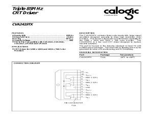
TX 1,6,8 Vin D1 C2 VCC L1 3,4,10 OUTPUT Vout R5 R4 CL D2 5 GND C1 = 0.01m F C2 = 1.0m F C3 = 0.1m F C4 = 0.47m F CL = 12pF (Including Parasitics) C6 = 1.0m F R1 = 7.5K R2 = 7.5K R3 = 10.0K R4 = 34 R5 = 5.1K R6 = 180 D1 = FDH400 D2 = FDH400 L1 = 560nH Q1 = 2N5770 1T-31 CALOGIC CORPORATION, 237 Whitney Place, Fremont, California 94539, Telephone: 510-656-2900, FAX: 510-651-1076 CVA2419TX CORPORATION APPLICATION INFORMATION FIGURE 2. CVA2419TX DC Characteristics The CVA2419TX is a high voltage triple CRT driver suitable for VGA, Super VGA, IBM 8514 1280 x 1024 and 1024 x 768 non-interlaced display applications. The CVA2419TX features 80V operation and low power dissipation. The part is housed in the industry standard 11 lead TO-220 molded power package. The heat sink is floating and may be grounded for ease of manufacturing and RFI shielding. Thermal Considerations The transfer characteristics of the amplifier are shown in Figure 2. Since this is a class A input stage, power supply current increases
 4 Pages, 46 KB, Original
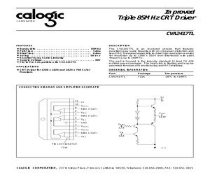
8 VIN D1 L1 3,4,10 VOUT R5 C2 VCC OUTPUT R4 CL D2 5 GND C1 = 0.01m F C2 = 0.01m F C3 = 0.1m F C4 = 0.47m F CL = 12pF (Including Parasitics) C6 = 1.0m F R1 = 8.2kW R2 = 2.7kW R3 = 10.0KW R4 = 34W R5 = 1.5kW R6 = 150W D1 = FDH400 D2 = FDH400 L1 = 560nH Q1 = 2N5770 1L-06 CALOGIC CORPORATION, 237 Whitney Place, Fremont, California 94539, Telephone: 510-656-2900, FAX: 510-651-3025 CVA2417TL CORPORATION APPLICATION INFORMATION FIGURE 2. CVA2417TL DC Characteristics The CVA2417TL is a high voltage triple CRT driver suitable for VGA, Super VGA, IBM(R) 8514, 1280 x 1024 and 1024 x 768 non-interlaced display applications. The CVA2417TL features 80V operation and low power dissipation. The part is housed in the industry standard 11 lead TO-220 molded power package. The heat sink is floating and may be grounded for ease of manufacturing and RFI shielding. Thermal Considerations The transfer characteristics of the amplifier are shown in Figure 2. Since this is a class A input stage, power supply current incre
 4 Pages, 35 KB, Original


