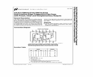
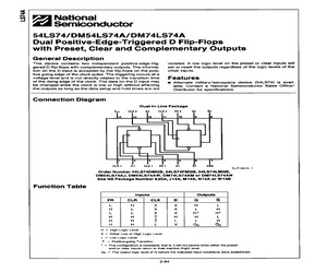
lock. The data on the D input may be changed while the clock is low or high without affecting the outputs as long as the data setup and hold times are not TL/F/6373 - 1 Order Number 54LS74DMQB, 54LS74FMQB, 54LS74LMQB, DM54LS74AJ, DM54LS74AW, DM74LS74AM or DM74LS74AN See NS Package Number E20A, J14A, M14A, N14A or W14B Function Table O Inputs Outputs PR CLR CLK D Q Q L H L H H H H L L H H H X X X X X X H L X H L H* H L Q0 L H H* L H Q0 u u L H e High Logic Level X e Either Low or High Logic Level L e Low Logic Level u e Positive-going Transition * e This configuration is nonstable; that is, it will not persist when either the preset and/or clear inputs return to their inactive (high) level. Q0 e The output logic level of Q before the indicated input conditions were established. C1995 National Semiconductor Corporation TL/F/6373 RRD-B30M105/Printed in U. S. A. 54LS74/DM54LS74A/DM74LS74A Dual Positive-Edge-Triggered D Flip-Flops with Preset, Clear and Complementary Outputs June 1989 Absolute Maximum
 8 Pages, 363 KB, Original
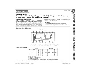
as the data setup and Connection Diagram Dual-In-Line Package Vee CLR2 b2 CLK2 PR2 az a2 14 13 12 iW lo a 8 > | > y | 1 2 3 4 5 6 7 CLR1 01 CLK1 PRI a a GND DS006373-1 Order Number 54LS74DMQGB, 54LS74FMQB, 54LS74LMQB, DM54LS74AJ, DM54LS74AW, DM74LS74AM or DM74LS74AN See Package Number E20A, J14A, M14A, N14A or W14B Function Table Inputs Outputs PR CLR CLK D Q Qa L H x x H L H L x x L H L L x x H (Note 1) _-H (Note 1) H H t H H H H t L L H H H L X Qo Qo H = High Logic Level X = Either Low or High Logic Level L = Low Logic Level t = Positive-going Transition Qo = The output logic level of Q before the indicated input conditions were established. Note 1: This configuration is nonstable; that is, it will not persist when either the preset and/or clear inputs return to their inactive (high) level. 1998 Fairchild Semiconductor Corporation | DS006373 www fairchildsemi.com sindino Asequawajdwoy pue e835 jaSaj1g yUM sdoj4-dij4 gq pasbbu-a6pz-aanisog jeng WrZS1rZINGAbsolute Maximum Ratings (noie 2) DM54LS
 6 Pages, 273 KB, Scan
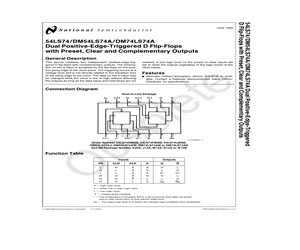
erospace device (54LS74) is available. Contact a Fairchild Semiconductor Sales Office/Distributor for specifications. Connection Diagram Dual-In-Line Package DS006373-1 Order Number 54LS74DMQB, 54LS74FMQB, 54LS74LMQB, DM54LS74AJ, DM54LS74AW, DM74LS74AM or DM74LS74AN See Package Number E20A, J14A, M14A, N14A or W14B Function Table Inputs Outputs PR CLR CLK D Q L H X X H Q L H L X X L H H (Note 1) L L X X H (Note 1) H H H H L H H L L H H H L X Q0 Q0 H = High Logic Level X = Either Low or High Logic Level L = Low Logic Level = Positive-going Transition Q0 = The output logic level of Q before the indicated input conditions were established. Note 1: This configuration is nonstable; that is, it will not persist when either the preset and/or clear inputs return to their inactive (high) level. (c) 1998 Fairchild Semiconductor Corporation DS006373 www.fairchildsemi.com DM74LS74A Dual Positive-Edge-Triggered D Flip-Flops with Preset, Clear and Complementary Outputs March 1998 Absolute Maximum Ratings (Note
 6 Pages, 117 KB, Original
lock. The data on the D input may be changed while the clock is low or high without affecting the outputs as long as the data setup and hold times are not TL/F/6373 - 1 Order Number 54LS74DMQB, 54LS74FMQB, 54LS74LMQB, DM54LS74AJ, DM54LS74AW, DM74LS74AM or DM74LS74AN See NS Package Number E20A, J14A, M14A, N14A or W14B Function Table O Inputs Outputs PR CLR CLK D Q Q L H L H H H H L L H H H X X X X X X H L X H L H* H L Q0 L H H* L H Q0 u u L H e High Logic Level X e Either Low or High Logic Level L e Low Logic Level u e Positive-going Transition * e This configuration is nonstable; that is, it will not persist when either the preset and/or clear inputs return to their inactive (high) level. Q0 e The output logic level of Q before the indicated input conditions were established. C1995 National Semiconductor Corporation TL/F/6373 RRD-B30M105/Printed in U. S. A. 54LS74/DM54LS74A/DM74LS74A Dual Positive-Edge-Triggered D Flip-Flops with Preset, Clear and Complementary Outputs June 1989 Absolute Maximum
 6 Pages, 326 KB, Original
tributor for specifications. Connection Diagram Dual-In-Line Package Vcc CLR2 D2 CLK2 = PR2 a2 a2 14 13 12 I le I. a > | 1 2 3 4 | cLR1 01 CLK1 PRI ai ai GND DS006373-1 Order Number 54LS74DMQB, 54LS74FMQB, 54LS74LMQB, DM54LS74AJ, DM54LS74AW, DM74LS74AM or DM74LS74AN See Package Number E20A, J14A, M14A, N14A or W14B Function Table Inputs Outputs PR CLR CLK D Q Q L H x x H L H L x x L H L L x x H (Note 1) H (Note 1) H H t H H L H H t L L H H H L x Qo Q H = High Logic Level X = Either Low or High Logic Level L = Low Logic Level t = Positive-going Transition Qo = The output logic level of Q before the indicated input conditions were established. Note 1: This configuration is nonstable; that is, it will not persist when either the preset and/or clear inputs return to their inactive (high) level. 1998 Fairchild Semiconductor Corporation DS006373 www fairchildsemi.com sindjino Axequawajdwoy pue J1e3]5 jaSsaig uM Sdoj4-dij4 gq paebbiup-a6bpz-aaisog jeng WrZS1rZINGAbsolute Maximum Ratings (noite 2) DMS54L
 6 Pages, 158 KB, Scan
space device (54LS74) is available. Contact a National Semiconductor Sales Office/ Distributor for specifications. Connection Diagram Dual-In-Line Package TL/F/6373 - 1 Order Number 54LS74DMQB, 54LS74FMQB, 54LS74LMQB, DM54LS74AJ, DM54LS74AW, DM74LS74AM or DM74LS74AN See NS Package Number E20A, J14A, M14A, N14A or W14B Function Table Inputs Outputs PR CLR CLK D Q Q L H L H H H H L L H H H X X X X X X H L X H L H* H L Q0 L H H* L H Q0 u u L H e High Logic Level X e Either Low or High Logic Level L e Low Logic Level u e Positive-going Transition * e This configuration is nonstable; that is, it will not persist when either the preset and/or clear inputs return to their inactive (high) level. Q0 e The output logic level of Q before the indicated input conditions were established. C1995 National Semiconductor Corporation TL/F/6373 RRD-B30M105/Printed in U. S. A. 54LS74/DM54LS74A/DM74LS74A Dual Positive-Edge-Triggered D Flip-Flops with Preset, Clear and Complementary Outputs June 1989 Absolute Maximum R
 6 Pages, 119 KB, Original
4MTCX 74AC74PC 74AC74SC 74AC74SCX 74AC74SJ 74AC74SJX 74ACT74SC 74ACTQ74SC DM74ALS74AM 74FR74PC 74FR74SC 74FR74SCX MM74HC74AM MM74HC74AMX MM74HC74N MM74HCT74N 74LCX74M 74LCX74MTC 74LCX74MTCX 74LCX74MX 74LCX74SJ 74LCX74SJX DM74LS74ACW DM74LS74AM DM74LS74AMX DM74LS74AN TI Orderable Not available Not available SN74LS38D SN74LS38DR SN74LS38N SN74LS38NSR SN74LS38NSR SN74S38NSR SN7438D SN7438DR SN7438N Not available Not available Not available Not available Not available Not available Not available SN7445N Not available SN74LS47D SN74LS47DR SN74LS47N SN7447AN Not available Not available Not available Not available Not available SN74LS51D SN74LS51DR SN74LS51N SN74S51N Not available Not available Not available Not available Not available Not available Not available SN74LS73AD SN74LS73AN Not available SN74F74N SN74F74N SN74F74D SN74F74D SN74F74DR SN74F74NSR SN74F74NSR SN74AC74PWR SN74AC74PWR SN74AC74N SN74AC74D SN74AC74DR SN74AC74NSR SN74AC74NSR SN74ACT74D Substitute SN74ALS74AD Not available Not available
 313 Pages, 2889 KB, Original
4MTCX 74AC74PC 74AC74SC 74AC74SCX 74AC74SJ 74AC74SJX 74ACT74SC 74ACTQ74SC DM74ALS74AM 74FR74PC 74FR74SC 74FR74SCX MM74HC74AM MM74HC74AMX MM74HC74N MM74HCT74N 74LCX74M 74LCX74MTC 74LCX74MTCX 74LCX74MX 74LCX74SJ 74LCX74SJX DM74LS74ACW DM74LS74AM DM74LS74AMX DM74LS74AN TI Orderable Not available Not available SN74LS38D SN74LS38DR SN74LS38N SN74LS38NSR SN74LS38NSR SN74S38NSR SN7438D SN7438DR SN7438N Not available Not available Not available Not available Not available Not available Not available SN7445N Not available SN74LS47D SN74LS47DR SN74LS47N SN7447AN Not available Not available Not available Not available Not available SN74LS51D SN74LS51DR SN74LS51N SN74S51N Not available Not available Not available Not available Not available Not available Not available SN74LS73AD SN74LS73AN Not available SN74F74N SN74F74N SN74F74D SN74F74D SN74F74DR SN74F74NSR SN74F74NSR SN74AC74PWR SN74AC74PWR SN74AC74N SN74AC74D SN74AC74DR SN74AC74NSR SN74AC74NSR SN74ACT74D Substitute SN74ALS74AD Not available Not available
 379 Pages, 3043 KB, Original
4MTCX 74AC74PC 74AC74SC 74AC74SCX 74AC74SJ 74AC74SJX 74ACT74SC 74ACTQ74SC DM74ALS74AM 74FR74PC 74FR74SC 74FR74SCX MM74HC74AM MM74HC74AMX MM74HC74N MM74HCT74N 74LCX74M 74LCX74MTC 74LCX74MTCX 74LCX74MX 74LCX74SJ 74LCX74SJX DM74LS74ACW DM74LS74AM DM74LS74AMX DM74LS74AN TI Orderable Not available Not available SN74LS38D SN74LS38DR SN74LS38N SN74LS38NSR SN74LS38NSR SN74S38NSR SN7438D SN7438DR SN7438N Not available Not available Not available Not available Not available Not available Not available SN7445N Not available SN74LS47D SN74LS47DR SN74LS47N SN7447AN Not available Not available Not available Not available Not available SN74LS51D SN74LS51DR SN74LS51N SN74S51N Not available Not available Not available Not available Not available Not available Not available SN74LS73AD SN74LS73AN Not available SN74F74N SN74F74N SN74F74D SN74F74D SN74F74DR SN74F74NSR SN74F74NSR SN74AC74PWR SN74AC74PWR SN74AC74N SN74AC74D SN74AC74DR SN74AC74NSR SN74AC74NSR SN74ACT74D Substitute SN74ALS74AD Not available Not available
 329 Pages, 2106 KB, Original
s. Connection Diagram Vee CLRZ o2 14 13 12 CLK2 [yw Dual-In-Line Package PR2 o2 a2 |, |. = Tle cits 1 2 a CLA 1 o1 CLK1 Function Table PRI ai a1 4 5 6 7 GND TL/F/6373-1 Order Number 54LS74DMQB, 54LS74FMQB, 54LS74LMQB, DM54LS74AJ, DM54LS74AW, DM74LS74AM or DM74LS74AN See NS Package Number E20A, J14A, M14A, N14A or W14B = Low Logic Level T = Positive-going Transition Inputs Outputs PR CLR CLK D Q a L H xX xX H L H L xX xX L H L L xX xX H* H* H H T H H L H H T L L H H H L x Qo Q = High Logic Level H X = Either Low or High Logic Level L * = This configuration is nonstable; that is, it will not persist when either the preset and/or clear inputs retum to their inactive (high) level. Qo = The output logic level of Q before the indicated input conditions were established. 1995 National Semiconductor Corporation TL/F/6373 RRD-B30M105/Printed in U.S. A. sindjno Asejusawajdwoy pure 1eajD 4asaidg uM Sdo|4-dil4 Gg pe19661 1 -86pz-aaiisod [eng VWrZS1PZING/VWPZS1PSINNG/PZS 1sAbsolute Maximum Ratings (note) If M
 6 Pages, 286 KB, Scan
MX DM74LS574N DM74LS574WM DM74LS574WMX DM74LS645N DM74LS645N DM74LS645WM DM74LS645WM DM74LS645WMX DM74LS670M DM74LS670MX DM74LS670N DM74LS73AM DM74LS73AM DM74LS73AM DM74LS73AMX DM74LS73AN DM74LS73AN DM74LS73AN DM74LS74AM DM74LS74AM DM74LS74AMX DM74LS74AMX DM74LS74AN DM74LS74ASJ DM74LS74ASJX DM74LS75M DM74LS75MX DM74LS75N DM74LS85M Competitor Fairchild Semiconductor Fairchild Semiconductor Fairchild Semiconductor Fairchild Semiconductor Fairchild Semiconductor Fairchild Semiconductor Fairchild Semiconductor Fairchild Semiconductor National Semiconductor (NSC) National Semiconductor (NSC) Fairchild Semiconductor Fairchild Semiconductor National Semiconductor (NSC) National Semiconductor (NSC) National Semiconductor (NSC) National Semiconductor (NSC) Fairchild Semiconductor Fairchild Semiconductor Fairchild Semiconductor Fairchild Semiconductor Fairchild Semiconductor Fairchild Semiconductor Fairchild Semiconductor Fairchild Semiconductor Fairchild Semiconductor Fairchild Semiconductor Fairchild Sem
 441 Pages, 3298 KB, Original
A1774S 12.88 CXA1908S 51.03 CXA2025AS 8.17 CXA2043Q 36.39 CXA2061S 19.17 CXA2095S 20.35 D40K1 8.60 DAC7545LU 15.79 DB104S 0.94 DB105G 1.59 DHD-1.5X2 92.89 DM463 0.79 DM7407N 0.90 DM74LS00N 0.60 DM74LS04N 0.53 DM74LS14N 0.87 DM74LS244N 1.41 DM74LS245N 1.61 DM74LS74AN 1.01 DS1216C 38.22 DS1230Y-150 26.64 DS1230Y-200 26.62 DS1243Y-120 20.90 DS1245AB-120 37.45 DS1245Y-100 37.45 DS1245Y-70 37.50 DS1267S-010 4.55 DS1621S 3.56 DS1687-5 10.62 DS2430A 3.40 DS446 0.06 DS5000-32-16 59.38 DS5000T-32-16 138.47 DS87C520-QCL 42.30 DS87C520-QNL 48.84 DS87C520-WCL 70.49 DS87C530-QCL 47.33 DTA114ES 0.30 DTA114YUA 0.49 DTA124EA 0.76 DTA124EK 0.49 DTA124ES 0.30 DTA124EUA 0.25 DTA143ES 0.57 DTA144EK 1.71 DTA144ES 0.30 DTB123ES 0.99 DTC114EA 0.15 DTC114EK* 0.30 DTC114ES 0.30 DTC124EF 0.93 DTC124EK* 2.24 DTC124ES 0.30 DTC143ES 0.30 DTC144ES 0.30 EF6821P 7.99 EP15X0223 8.10 EP84X0215 8.51 ES1F 1.61 EW02X0408 6.93 EW02X0752 2.51 FDS6982S 1.92 FEP16JT 2.21 FES8GT 1.85 FH340M 7.19 FN1016 3.99 FP1016 4.20 Order # (1-9) FR10
 31 Pages, 2754 KB, Original
12.16 19.87 12.44 14.73 15.96 12.49 13.39 11.84 21.14 13.52 11.58 12.22 12.17 13.12 13.30 16.46 11.43 100 40.08 39.63 42.82 68.24 38.33 39.25 44.82 38.71 40.17 66.95 41.12 49.61 53.76 42.08 45.10 39.11 71.19 45.53 38.25 40.39 40.21 44.20 44.80 55.45 38.50 DM74LS74AN-ND Dual D Type Flip Flop w/Set & Reset . . . . . . . . . . . . . . . . . . . 14-Dip DM74LS75N-ND Quad Latch . . . . . . . . . . . . . . . . . . . . . . . . . . . . . . . . . . . . . . . . . . . . . 16-Dip DM74LS83AN-ND 4-Bit Binary Full Adder . . . . . . . . . . . . . . . . . . . . . . . . . . . . . . . . . 16-Dip DM74LS85N-ND 4-Bit Magnitude Comparator . . . . . . . . . . . . . . . . . . . . . . . . . . . 16-Dip DM74LS86N-ND Quad 2-Input Exclusive OR Gate . . . . . . . . . . . . . . . . . . . . . . . 14-Dip DM74LS90N-ND Decade Counter . . . . . . . . . . . . . . . . . . . . . . . . . . . . . . . . . . . . . . . . 14-Dip DM74LS109AN-ND Dual JK Flip Flop . . . . . . . . . . . . . . . . . . . . . . . . . . . . . . . . . . . . . . . 16-D
 531 Pages, 19076 KB, Original
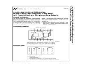
 of the other inputs. Ordering Code: Order Number Package Number Package Description DM74LS74AM M14A 14-Lead Small Outline Integrated Circuit (SOIC), JEDEC MS-120, 0.150 Narrow DM74LS85ASJ M14D 14-Lead Small Outline Package (SOP), EIAJ TYPE II, 5.3mm Wide DM74LS74AN N14A 14-Lead Plastic Dual-In-Line Package (PDIP), JEDEC MS-001, 0.300 Wide Devices also available in Tape and Reel. Specify by appending the suffix letter "X" to the ordering code. Connection Diagram Function Table Inputs Outputs PR CLR CLK D Q L H X X H Q L H L X X L H L L X X H H H H (Note 1) H (Note 1) H L H H L L H H H L X Q0 Q0 H = HIGH Logic Level X = Either LOW or HIGH Logic Level L = LOW Logic Level = Positive-going Transition Q0 = The output logic level of Q before the indicated input conditions were established. Note 1: This configuration is nonstable; that is, it will not persist when either the preset and/or clear inputs return to their inactive (HIGH) level. (c) 2000 Fairchild Semiconductor Corporation DS006373 www.fairch
 6 Pages, 59 KB, Original
tributor for specifications. Connection Diagram Dual-In-Line Package Veco CLR2 D2 CLK2-PR2 a2 iF] 14 13 nz a1 10 9 is > 0 1 2 3 | cLR1 D1 CLKt PRI a1 at GND TL/F/6373~1 Order Number 54LS74DMQB, 54LS74FMQB, 54LS74LMQB, DM54LS74AJ, DM54LS74AW, DM74LS74AM or DM74LS74AN See NS Package Number E20A, J14A, M14A, N14A or W148 Function Table Inputs CLR CLK rrIirmeire TrIrmreet ral KK XK Outputs D Q a xX H L xX L H Xx H* H* H H L L L H X Qo Go H = High Logic Level X = Either Low or High Logic Level L = Low Logic Level T = Positive-going Transition * = This configuration is nonstable; that is, it will not parsist when either the preset and/or clear inputs return to their inactive (high) lavei. Qo = The output logic level of Q before the indicated input conditions were established. 2-84Absolute Maximum Ratings (note) \f Military/Aerospace specified devices are required, please contact the National Semiconductor Sales Office/Distributors for availability and specifications. Supply Voltage 7V Input Voltage 7V
 3 Pages, 91 KB, Scan


