t Voltage: 0.75V at 3A +1% Reference Voltage Accurate Programmable Current Limit Shutdown Capability Internal Reference Available Standard 5-Lead Packages Full Remote Sense Low Quiescent Current: =2.5mA Good High Frequency Ripple Rejection DESCRIPTION The LT1185 is a 3A low dropout regulator with adjustable current limit and remote sense capability. It can be used as a positive output regulator with floating input or as a Standard negative regulator with grounded input. The output voltage range is 2.5Vto 25V, with+1% accuracy on the internal reference voltage. nt AR LT1185 Low Dropout Regulator The LT1185 uses a saturation-limited NPN transistor as the pass element. This device gives the linear dropout characteristics of an FET pass element with significantly less die area. High efficiency is maintained by using special anti-saturation circuitry that adjusts base drive to track load current. The on resistance is typically 0.25Q. Accurate current limit is programmed with
 16 Pages, 618 KB, Scan
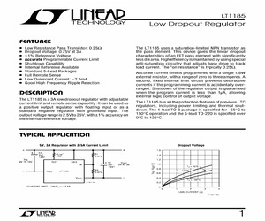
LT1185 Low Dropout Regulator FEATURES The LT1185 uses a saturation-limited NPN transistor as the pass element. This device gives the linear dropout characteristics of an FET pass element with significantly less die area. High efficiency is maintained by using special anti-saturation circuitry that adjusts base drive to track load current. The "on resistance" is typically 0.25. Low Resistance Pass Transistor: 0.25 Dropout Voltage: 0.75V at 3A 1% Reference Voltage Accurate Programmable Current Limit Shutdown Capability Internal Reference Available Standard 5-Lead Packages Full Remote Sense Low Quiescent Current: 2.5mA Good High Frequency Ripple Rejection U DESCRIPTIO The LT(R)1185 is a 3A low dropout regulator with adjustable current limit and remote sense capability. It can be used as a positive output regulator with floating input or as a standard negative regulator with grounded input. The output voltage range is 2.5V to 25V, with 1% accuracy on the internal reference voltage. Accur
 16 Pages, 215 KB, Original
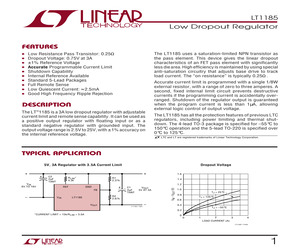
LT1185 Low Dropout Regulator FEATURES Low Resistance Pass Transistor: 0.25 Dropout Voltage: 0.75V at 3A 1% Reference Voltage Accurate Programmable Current Limit Shutdown Capability Internal Reference Available Standard 5-Lead Packages Full Remote Sense Low Quiescent Current: 2.5mA Good High Frequency Ripple Rejection The LT1185 uses a saturation-limited NPN transistor as the pass element. This device gives the linear dropout characteristics of an FET pass element with significantly less die area. High efficiency is maintained by using special anti-saturation circuitry that adjusts base drive to track load current. The "on resistance" is typically 0.25. U DESCRIPTIO The LT1185 is a 3A low dropout regulator with adjustable current limit and remote sense capability. It can be used as a positive output regulator with floating input or as a standard negative regulator with grounded input. The output voltage range is 2.5V to 25V, with 1% accuracy on the internal reference volt
 16 Pages, 230 KB, Original
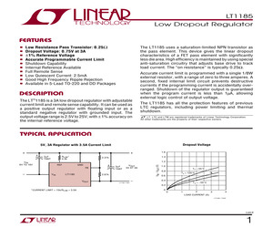
LT1185 Low Dropout Regulator FEATURES Low Resistance Pass Transistor: 0.25 Dropout Voltage: 0.75V at 3A 1% Reference Voltage Accurate Programmable Current Limit Shutdown Capability Internal Reference Available Full Remote Sense Low Quiescent Current: 2.5mA Good High Frequency Ripple Rejection Available in 5-Lead TO-220 and DD Packages The LT1185 uses a saturation-limited NPN transistor as the pass element. This device gives the linear dropout characteristics of a FET pass element with significantly less die area. High efficiency is maintained by using special anti-saturation circuitry that adjusts base drive to track load current. The "on resistance" is typically 0.25. U DESCRIPTIO The LT(R)1185 is a 3A low dropout regulator with adjustable current limit and remote sense capability. It can be used as a positive output regulator with floating input or as a standard negative regulator with grounded input. The output voltage range is 2.5V to 25V, with 1% accuracy on the internal referen
 16 Pages, 180 KB, Original
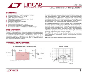
LT1185 Low Dropout Regulator FEATURES The LT1185 uses a saturation-limited NPN transistor as the pass element. This device gives the linear dropout characteristics of a FET pass element with significantly less die area. High efficiency is maintained by using special anti-saturation circuitry that adjusts base drive to track load current. The "on resistance" is typically 0.25. Low Resistance Pass Transistor: 0.25 Dropout Voltage: 0.75V at 3A 1% Reference Voltage Accurate Programmable Current Limit Shutdown Capability Internal Reference Available Full Remote Sense Low Quiescent Current: 2.5mA Good High Frequency Ripple Rejection Available in 5-Lead TO-220 and DD Packages U DESCRIPTIO The LT(R)1185 is a 3A low dropout regulator with adjustable current limit and remote sense capability. It can be used as a positive output regulator with floating input or as a standard negative regulator with grounded input. The output voltage range is 2.5V to 25V, with 1% accuracy on the internal referen
 16 Pages, 220 KB, Original
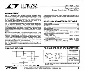
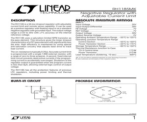
LT1185M/883 TECHNOLOGY DESCRIPTION The LT1185M/883 is a 3A low dropout regulator with adjustable current limit and remote sense capability. It can be used as a positive output regulator with floating input or as a Standard negative regulator with grounded input. The output voltage range is 2.5V to 25V, with +1% accuracy on the internal reference voltage. The LT1185M/883 uses a saturation-limited NPN transis- tor as the pass element. This device gives the linear dropout characteristics of an FET pass element with sig- nificantly less die area. High efficiency is maintained by using special anti-saturation circuitry that adjusts base drive to track load current. The on resistance is typically 0.25Q. Accurate current limit is programmed with a single 1/8W external resistor, with a range of zero to three amperes. A second, fixed internal limit circuit prevents destructive currents if the programming current is accidentally over- ranged. Shutdown of the regulator output is gu
 3 Pages, 253 KB, Scan
 Publication Page Number Figure Number Ultraprecision (Continued) Publication Page Number Category LT1020 DS 12 NA LT1020 DN82 1 2 LT1085 DN82 1 1 LT1085, LTC1157 Current Limited 1A Regulator LT1020 DS 12 NA LT1020 Improved High Frequency Ripple Rejection LT1185 DS 14 NA LT1185 LT138 DS 7 NA LT338A LT1038 DS 8 NA LT1038 LT1009 DS 4 NA LT1009, LT317A Pin-Switchable 3.3V/5V Regulator Configuration AN58 3 2 (see text) Pin-Switchable 3.3V/5V Regulator Configuration with LTC1157 AN58 3 3 LT1157 and linear regulator (see text) Subject Ultraprecision Variable Voltage Reference LT Part Number(s) Regulators--Linear Category Subject Additional 1A Regulator with Current Limit Feature Circuits Bypass Circuit for 3.xxV and 5V Microprocessor Swaps Using High-Side Gate Driver Bypass Circuit for 3.xxV and 5V Microprocessor Swaps with Transistor Buffer LT Part Number(s) Improving Ripple Rejection Low Temperature Coefficient Power Regulator 105 SUBJECT INDEX Regulators--Linear (Continued) Publication
 177 Pages, 1074 KB, Original
 network clamps the flyback voltage spike, AN46-12Application Note 46 (E13) Voyr = 2.74 (1+ 212 ) ) (E014) Voyry = 2.57V (1 + BS Figure 30. LT1070 Flyback Switching Regulator De eit MUR110 J | gutz 12V < LT1185 i Vout . MUR110 aa L = S8um"" S74 > 15k > 2.37k* * = 1% FILM RESISTORS Lt pour ** = CURRENT LIMIT = (154/B)1y4) A REF GND TANTALUM Lt = COILTRONICS - CTX02-11808-1 FB TANTALU L2 = COILTRONICS - CTX5-5-FR ; = MOTOROLA - MBR745 71485 $R3 D2 = MOTOROLA - MUR110 9.76k D3 = MOTOROLA - P6KE36A C1 = NICHICON - UPL1E471MRH6 y NVour C2, C3 = NICHICON - UPL1A222MRH6 out -* -12V Gd = NICHICON - UPL1A221 MPH C5, CB = NICHICON - UPL1E471MPH D3 2 MBR745 5yH ; . >t orrrn Vout vw 5V 4A 2) @Vyy 2 12V D4 3 36V 5W c2 4 03 4 C4 + C1 e 2200uF 2200uF == 220uF = 470uF muro 2 0 10V 10V 10v eat < * 26v U1 > 3.01k Vin Vow -# + LT1070 Veg GNO Ve ti, = 3WLoov J. 1k > 1.00k" T 0.33,F - RL (E012) Voyr = 1.24V (1+ at 1) LTAN46 + TA30 AN46-13Application Note 46 A= 50WDI
 28 Pages, 2569 KB, Scan
atings, typical specifications, performance curves and finished product specifications, please refer to the standard product RH data sheet. UNITS Note 2: Testing is done using a pulsed low duty cycle technique. See thermal regulation specifications in the LT1185 data sheet for output changes due to heating effects. Information furnished by Linear Technology Corporation is believed to be accurate and reliable. However, no responsibility is assumed for its use. Linear Technology Corporation makes no representation that the interconnection of its circuits as described herein will not infringe on existing patent rights. 1 DICE/DWF SPECIFICATION RH1185MK DICE/DWF ELECTRICAL TEST LIMITS VIN = 7.4V, VOUT = 5V, IOUT = 1mA, RLIM = 4.02k, unless otherwise noted. Note 3: Dropout voltage is tested by reducing input voltage until the output drops 1% below its nominal value. Tests are done at 0.5A and 3A. The power transistor looks basically like a pure resistance in this range so that minimum differential at
 2 Pages, 61 KB, Original
teed by design and correlation to other tests, but not tested. 9. TJMIN = - 40C for AS1185I and -55C for the AS1185M. Power transistor area and control circuit area have different maximum junction temperatures. Control area limits are TJMAX = 125C for the LT1185C and LT1185I and 150C for the LT1185M. Power area limits are 150C for AS1185I and 175C for AS1185M. 10. VSAT is the maximum specified dropout voltage; 0.25V + 0.25 * IOUT. 11. Current limit is programmed with a resistor from REF pin to GND pin. The value is 15k/ILIM. 12. For VIN - VOUT = 1.5V; VIN = 5V, VOUT = 3.5V. VOUT = 1V for all other current limit tests. AS1185 Rev. 1.0 6/03 Austin Semiconductor, Inc. reserves the right to change products or specifications without notice. 2 LOW DROPOUT REGULA TOR REGULAT Austin Semiconductor, Inc. AS1185 ELECTRICAL CHARACTERISTICS: The * denotes specifications which apply over the operating temperature range, otherwise specifications are at TA = 25C. Adjustable version, VIN
 7 Pages, 110 KB, Original
The power transistor looks basically like a pure resistance in this range so that minimum differential at any intermediate current can be calculated by interpolation; VDROPOUT = 0.25V + 0.25 * IOUT . For load current other than 0.5A and 3.0A, see graph in LT1185 data sheet. Note 4: "Minimum input voltage" is limited by base emitter voltage drive of the power transistor section, not saturation as measured in Note 3. For output voltages below 4V, "minimum input voltage" specification may limit dropout voltage before transistor saturation limitation. Note 5: Supply current is measured on the ground pin, and does not include load current, RLIM, or output divider current. 7 5 1 Note 6: The 25W power level is guaranteed for an input-output voltage of 8.3V to 17V. At lower voltages the 3A limit applies, and at higher voltages the internal power limiting may restrict regulator power below 25W. See graph of Internal Current Limit in LT1185 data sheet. Note 7: Line and load regulation are meas
 6 Pages, 79 KB, Original
atings, typical specifications, performance curves and finished product specifications, please refer to the standard product RH data sheet. UNITS Note 2: Testing is done using a pulsed low duty cycle technique. See thermal regulation specifications in the LT1185 data sheet for output changes due to heating effects. Information furnished by Linear Technology Corporation is believed to be accurate and reliable. However, no responsibility is assumed for its use. Linear Technology Corporation makes no representation that the interconnection of its circuits as described herein will not infringe on existing patent rights. 1 DICE/DWF SPECIFICATION RH1185MK DICE/DWF ELECTRICAL TEST LIMITS VIN = 7.4V, VOUT = 5V, IOUT = 1mA, RLIM = 4.02k, unless otherwise noted. Note 3: Dropout voltage is tested by reducing input voltage until the output drops 1% below its nominal value. Tests are done at 0.5A and 3A. The power transistor looks basically like a pure resistance in this range so that minimum differential at
 2 Pages, 90 KB, Original
atings, typical specifications, performance curves and finished product specifications, please refer to the standard product RH data sheet. UNITS Note 2: Testing is done using a pulsed low duty cycle technique. See thermal regulation specifications in the LT1185 data sheet for output changes due to heating effects. Information furnished by Linear Technology Corporation is believed to be accurate and reliable. However, no responsibility is assumed for its use. Linear Technology Corporation makes no representation that the interconnection of its circuits as described herein will not infringe on existing patent rights. 1 DICE/DWF SPECIFICATION RH1185MK DICE/DWF ELECTRICAL TEST LIMITS VIN = 7.4V, VOUT = 5V, IOUT = 1mA, RLIM = 4.02k, unless otherwise noted. Note 3: Dropout voltage is tested by reducing input voltage until the output drops 1% below its nominal value. Tests are done at 0.5A and 3A. The power transistor looks basically like a pure resistance in this range so that minimum differential at
 2 Pages, 61 KB, Original
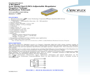
to MIL-STD-883, the VRG8663 is ideal for demanding military and space applications. For detailed performance characteristic curves, applications information and typical applications see the latest Linear Technology Corporation (R) data sheets for their RH/LT1185, which is available on-line at www.linear.com. 3 VOUT VIN 5 Reference 2 Feedback 1 RH1185 GND 4 FIGURE 1 - BLOCK DIAGRAM / SCHEMATIC SCD8663 Rev B ABSOLUTE MAXIMUM RATINGS PARAMETER RANGE UNITS Input Voltage -35 VDC Lead temperature (soldering 10 Sec) 300 C Input Output Differential -30 VDC Feedback & Reference Voltage -7 VDC Output Voltage -30 VDC 2000 1/ V Operating Junction Temperature Range -55 to +150 C Storage Temperature Range -65 to +150 C ESD NOTICE: Stresses above those listed under "Absolute Maximums Rating" may cause permanent damage to the device. These are stress rating only; functional operation beyond the "Operation Conditions" is not recommended and extended exposure beyond the "Operation Conditions" may effect device rel
 7 Pages, 294 KB, Original
 The power transistor looks basically like a pure resistance in this range so that minimum differential at any intermediate current can be calculated by interpolation; VDROPOUT = 0.25V + 0.25 * IOUT. For load current other than 0.5A and 3.0A, see graph in LT1185 data sheet. Note 4: "Minimum input voltage" is limited by base emitter voltage drive of the power transistor section, not saturation as measured in Note 3. For output voltages below 4V, "minimum input voltage" specification may limit dropout voltage before transistor saturation limitation. Note 5: Supply current is measured on the ground pin, and does not include load current, RLIM, or output divider current. Note 6: The 25W power level is guaranteed for an input-output voltage of 8.3V to 17V. At lower voltages the 3A limit applies, and at higher voltages the internal power limiting may restrict regulator power below 25W. See graph of Internal Current Limit in LT1185 data sheet. Note 7: Line and load regulation are measured o
 6 Pages, 393 KB, Original


