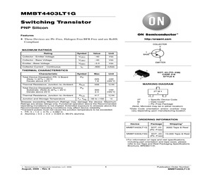
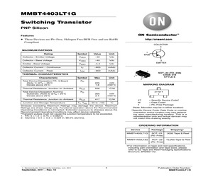
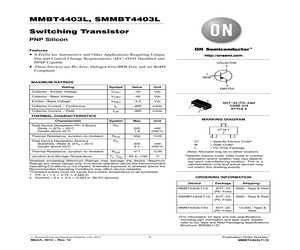
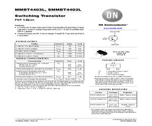
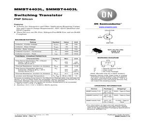
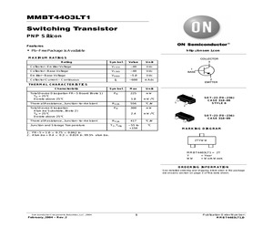
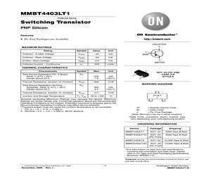
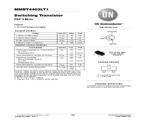
MMBT4403LT1G Switching Transistor PNP Silicon Features * These Devices are Pb-Free, Halogen Free/BFR Free and are RoHS http://onsemi.com Compliant COLLECTOR 3 MAXIMUM RATINGS Rating Symbol Value Unit Collector -Emitter Voltage VCEO -40 Vdc Collector -Base Voltage VCBO -40 Vdc Emitter -Base Voltage VEBO -5.0 Vdc Collector Current - Continuous Collector Current - Peak IC -600 mAdc ICM -900 mAdc Symbol Max Unit 225 1.8 mW mW/C 556 C/W 300 2.4 mW mW/C RqJA 417 C/W TJ, Tstg -55 to +150 C 1 BASE 2 EMITTER 3 SOT-23 (TO-236) CASE 318 STYLE 6 THERMAL CHARACTERISTICS Characteristic Total Device Dissipation FR- 5 Board (Note 1) @TA = 25C Derate above 25C Thermal Resistance, Junction-to-Ambient Total Device Dissipation Alumina Substrate, (Note 2) @TA = 25C Derate above 25C Thermal Resistance, Junction-to-Ambient Junction and Storage Temperature PD RqJA PD Stresses exceeding Maximum Ratings may damage the device. Maximum Ratings are stress ratings only. Functional operation above the Recommended Operating Con
 7 Pages, 145 KB, Original
MMBT4403LT1G Switching Transistor PNP Silicon Features * These Devices are Pb-Free, Halogen Free/BFR Free and are RoHS http://onsemi.com Compliant COLLECTOR 3 MAXIMUM RATINGS Rating Symbol Value Unit Collector -Emitter Voltage VCEO -40 Vdc Collector -Base Voltage VCBO -40 Vdc Emitter-Base Voltage VEBO -5.0 Vdc IC -600 mAdc Symbol Max Unit 225 1.8 mW mW/C 556 C/W 300 2.4 mW mW/C RqJA 417 C/W TJ, Tstg -55 to +150 C Collector Current - Continuous 1 BASE 2 EMITTER THERMAL CHARACTERISTICS Characteristic Total Device Dissipation FR- 5 Board (Note 1) @TA = 25C Derate above 25C Thermal Resistance, Junction-to-Ambient Total Device Dissipation Alumina Substrate, (Note 2) @TA = 25C Derate above 25C Thermal Resistance, Junction-to-Ambient Junction and Storage Temperature 3 PD RqJA PD SOT-23 (TO-236) CASE 318 STYLE 6 1 Stresses exceeding Maximum Ratings may damage the device. Maximum Ratings are stress ratings only. Functional operation above the Recommended Operating Conditions is not implied. Extended expos
 7 Pages, 197 KB, Original
MMBT4403LT1G Switching Transistor PNP Silicon Features * These Devices are Pb-Free, Halogen Free/BFR Free and are RoHS http://onsemi.com Compliant COLLECTOR 3 MAXIMUM RATINGS Rating Symbol Value Unit Collector -Emitter Voltage VCEO -40 Vdc Collector -Base Voltage VCBO -40 Vdc Emitter -Base Voltage VEBO -5.0 Vdc Collector Current - Continuous Collector Current - Peak IC -600 mAdc ICM -900 mAdc Symbol Max Unit 225 1.8 mW mW/C 556 C/W 300 2.4 mW mW/C RqJA 417 C/W TJ, Tstg -55 to +150 C 1 BASE 2 EMITTER 3 SOT-23 (TO-236) CASE 318 STYLE 6 THERMAL CHARACTERISTICS Characteristic Total Device Dissipation FR- 5 Board (Note 1) @TA = 25C Derate above 25C Thermal Resistance, Junction-to-Ambient Total Device Dissipation Alumina Substrate, (Note 2) @TA = 25C Derate above 25C Thermal Resistance, Junction-to-Ambient Junction and Storage Temperature PD RqJA PD Stresses exceeding Maximum Ratings may damage the device. Maximum Ratings are stress ratings only. Functional operation above the Recommended Operating Con
 7 Pages, 144 KB, Original
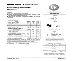
tion) *Specific Device Code, Date Code or overbar orientation and/or location may vary depending upon manufacturing location. This is a representation only and actual devices may not match this drawing exactly. ORDERING INFORMATION Device Package Shipping MMBT4403LT1G SOT-23 3000 / Tape & Reel (Pb-Free) SMMBT4403LT1G SOT-23 3000 / Tape & Reel (Pb-Free) MMBT4403LT3G SOT-23 (Pb-Free) 10,000 / Tape & Reel For information on tape and reel specifications, including part orientation and tape sizes, please refer to our Tape and Reel Packaging Specifications Brochure, BRD8011/D. (c) Semiconductor Components Industries, LLC, 1994 October, 2016 - Rev. 13 1 Publication Order Number: MMBT4403LT1/D MMBT4403L, SMMBT4403L ELECTRICAL CHARACTERISTICS (TA = 25C unless otherwise noted) Characteristic Symbol Min Max Unit OFF CHARACTERISTICS Collector -Emitter Breakdown Voltage (Note 3) (IC = -1.0 mAdc, IB = 0) V(BR)CEO -40 - Vdc Collector -Base Breakdown Voltage (IC = -0.1 mAdc, IE = 0) V(BR)CBO -40 - V
 8 Pages, 161 KB, Original
-BUL146FG 863-MJE13007G 863-MJE13009G 863-BUX85G 863-MJE18004G 863-MJE18008G PNP 863-BCP69T1G 863-MMBT4126LT1G 863-MPS4126RLRAG 863-MJD210G 863-MJE210G 863-BC858BLT1G 863-BC858CLT1G 863-2N6111G 863-2N3906G 863-MMBT3906LT1G 863-MMBT3906WT1G 863-2N4403G 863-MMBT4403LT1G 863-MJE371G 863-TIP42G 863-MMBT5087LT1G 863-BC857BLT1G 863-BC807-16LT1G 863-BC807-25LT1G 863-BC807-40LT1G 863-BCX17LT1G 863-2N6109G 863-2SA1774G 863-MPSA55RLRAG 863-MMBTA55LT1G 863-MMBT2907ALT1G 863-MMBT2907AWT1G 863-MPS2907AG 863-PZT2907AT1G 863-MPS751RLRAG 863-TIP32AG 863-MJE2955TG 863-2N5883G 863-2N6107G (c) Copyright 2011 Mouser Electronics 476 ON Semi Part No. TIP31BG MJD44H11G D44H11G MJF44H11G 2N6488G D44VH10G 2N5886G 2N5038G MJ802G TIP29CG MJD31CG TIP31CG MJE243G TIP41CG TIP33CG TIP35CG 2N3442G 2N3773G MJF15030G MMBT5551LT1G MJE4343G MJE344G MMBTA42LT1G BU406G 2N5655G TIP47G MJF47G MJE340G PZTA42T1G TIP48G MMBT6517LT1G 2N5657G TIP50G BUL45D2G BUL146FG MJE13007G MJE13009G BUX85G MJE18004G MJE18008G BCP69T1G MMBT4126LT1G MPS41
 379 Pages, 47721 KB, Original
tion) *Specific Device Code, Date Code or overbar orientation and/or location may vary depending upon manufacturing location. This is a representation only and actual devices may not match this drawing exactly. ORDERING INFORMATION Device Package Shipping MMBT4403LT1G SOT-23 3000 / Tape & Reel (Pb-Free) SMMBT4403LT1G SOT-23 3000 / Tape & Reel (Pb-Free) MMBT4403LT3G SOT-23 (Pb-Free) 10,000 / Tape & Reel For information on tape and reel specifications, including part orientation and tape sizes, please refer to our Tape and Reel Packaging Specifications Brochure, BRD8011/D. (c) Semiconductor Components Industries, LLC, 2011 November, 2011 - Rev. 11 1 Publication Order Number: MMBT4403LT1/D MMBT4403L, SMMBT4403L ELECTRICAL CHARACTERISTICS (TA = 25C unless otherwise noted) Characteristic Symbol Min Max Unit OFF CHARACTERISTICS Collector -Emitter Breakdown Voltage (Note 3) (IC = -1.0 mAdc, IB = 0) V(BR)CEO -40 - Vdc Collector -Base Breakdown Voltage (IC = -0.1 mAdc, IE = 0) V(BR)CBO -40 -
 7 Pages, 224 KB, Original
tion) *Specific Device Code, Date Code or overbar orientation and/or location may vary depending upon manufacturing location. This is a representation only and actual devices may not match this drawing exactly. ORDERING INFORMATION Device Package Shipping MMBT4403LT1G SOT-23 3000 / Tape & Reel (Pb-Free) SMMBT4403LT1G SOT-23 3000 / Tape & Reel (Pb-Free) MMBT4403LT3G SOT-23 (Pb-Free) 10,000 / Tape & Reel For information on tape and reel specifications, including part orientation and tape sizes, please refer to our Tape and Reel Packaging Specifications Brochure, BRD8011/D. (c) Semiconductor Components Industries, LLC, 2012 March, 2012 - Rev. 12 1 Publication Order Number: MMBT4403LT1/D MMBT4403L, SMMBT4403L ELECTRICAL CHARACTERISTICS (TA = 25C unless otherwise noted) Characteristic Symbol Min Max Unit OFF CHARACTERISTICS Collector -Emitter Breakdown Voltage (Note 3) (IC = -1.0 mAdc, IB = 0) V(BR)CEO -40 - Vdc Collector -Base Breakdown Voltage (IC = -0.1 mAdc, IE = 0) V(BR)CBO -40 - Vdc
 7 Pages, 141 KB, Original
601CF8T1G 863-NSS40301MZ4T1G 863-NSS60601MZ4T1G PNP 863-NSS12100UW3TCG 863-NSS12100XV6T1G 863-NSS20200LT1G 863-NSS40200LT1G 863-NSS40600CF8T1G NPN 863-MMBT918LT1G 863-MMBT2369ALT1G 863-MMBT2369LT1G 863-MMBTH10LT1G 863-MMBT4401LT1G 863-MMBT4401WT1G PNP 863-MMBT4403LT1G .062 .062 .067 .227 .067 1000 .042 .042 .046 .17 .046 15 20 25 30 25 30 10 25 10 16 10 15 20 15 20 25 20 15 20 15 70 60 100 60 100 100 100 75 70 - 6.15 4.35 3.93 4.15 3.93 3.93 1.69 2.53 6.15 3.34 4.94 3.49 3.15 3.53 3.15 3.15 1.43 2.15 4.94 2.84 4.51 3.18 2.87 3.06 2.87 2.87 1.15 1.72 4.51 2.46 3.06 2.16 1.95 2.19 1.95 1.95 .834 1.24 3.06 1.76 2N5883G 2N5884G 2N5684G TIP36CG TO-3 TO-3 TO-3 TO-218 -60 -80 -80 -100 -25 -25 -50 -25 20 20 15 15 100 100 60 75 3.93 4.29 8.73 2.63 3.34 3.45 7.89 2.24 2.90 3.14 6.53 1.79 2.07 2.13 4.78 1.29 SOT-23 SOT-23 SOT-23 25 30 60 0.05 0.05 0.1 400 300 250 1200 900 - MMBT5087LT1G SOT-23 -50 -0.05 250 800 Package .19 .21 .22 .179 .178 .147 .063 .063 .061 .042 .043 .042 SOT-23 SOT-223 .19 .179 .063 .04
 1 Pages, 248 KB, Original
tion) *Specific Device Code, Date Code or overbar orientation and/or location may vary depending upon manufacturing location. This is a representation only and actual devices may not match this drawing exactly. ORDERING INFORMATION Device Package Shipping MMBT4403LT1G SOT-23 3000 / Tape & Reel (Pb-Free) SMMBT4403LT1G SOT-23 3000 / Tape & Reel (Pb-Free) MMBT4403LT3G SOT-23 (Pb-Free) 10,000 / Tape & Reel For information on tape and reel specifications, including part orientation and tape sizes, please refer to our Tape and Reel Packaging Specifications Brochure, BRD8011/D. (c) Semiconductor Components Industries, LLC, 1994 October, 2016 - Rev. 13 1 Publication Order Number: MMBT4403LT1/D MMBT4403L, SMMBT4403L ELECTRICAL CHARACTERISTICS (TA = 25C unless otherwise noted) Characteristic Symbol Min Max Unit OFF CHARACTERISTICS Collector -Emitter Breakdown Voltage (Note 3) (IC = -1.0 mAdc, IB = 0) V(BR)CEO -40 - Vdc Collector -Base Breakdown Voltage (IC = -0.1 mAdc, IE = 0) V(BR)CBO -40 - V
 7 Pages, 159 KB, Original
tion) *Specific Device Code, Date Code or overbar orientation and/or location may vary depending upon manufacturing location. This is a representation only and actual devices may not match this drawing exactly. ORDERING INFORMATION Device Package Shipping MMBT4403LT1G SOT-23 3000 / Tape & Reel (Pb-Free) SMMBT4403LT1G SOT-23 3000 / Tape & Reel (Pb-Free) MMBT4403LT3G SOT-23 (Pb-Free) 10,000 / Tape & Reel For information on tape and reel specifications, including part orientation and tape sizes, please refer to our Tape and Reel Packaging Specifications Brochure, BRD8011/D. (c) Semiconductor Components Industries, LLC, 1994 October, 2016 - Rev. 13 1 Publication Order Number: MMBT4403LT1/D MMBT4403L, SMMBT4403L ELECTRICAL CHARACTERISTICS (TA = 25C unless otherwise noted) Characteristic Symbol Min Max Unit OFF CHARACTERISTICS Collector -Emitter Breakdown Voltage (Note 3) (IC = -1.0 mAdc, IB = 0) V(BR)CEO -40 - Vdc Collector -Base Breakdown Voltage (IC = -0.1 mAdc, IE = 0) V(BR)CBO -40 - V
 8 Pages, 222 KB, Original
 NPN 40V 2 3000 .0467 3000 MMBT4401LT3 A SS SOT23 GP XSTR NPN 40V 2 10000 .0467 10000 MMBT4401WT1 A SS SC70 GP XSTR NPN 40V 2 3000 .0427 3000 MMBT4401WT1G A SS SC70 GP XSTR NPN 40V 2 3000 .0427 3000 MMBT4403LT1 A SS SOT23 GP XSTR PNP 40V 2 3000 .0467 3000 MMBT4403LT1G A SS SOT23 GP XSTR PNP 40V 2 3000 .0467 3000 MMBT4403LT3 A SS SOT23 GP XSTR PNP 40V 2 10000 .0467 10000 MMBT4403WT1 A SS SC70 GP XSTR NPN 40V 2 3000 .0427 3000 MMBT4403WT1G A SS SC70 GP XSTR NPN 40V 2 3000 .0427 3000 MMBT489LT1 A SS SOT23 GP XSTR NPN 50V 2 3000 .24 3000 MMBT5087LT1 A SS SOT23 LN XSTR PNP 50V 2 3000 .0467 3000 MMBT5087LT1G A SS SOT23 LN XSTR PNP 50V 2 3000 .0467 3000 MMBT5087LT3 A SS SOT23 LN XSTR PNP 50V 2 10000 .0467 10000 MMBT5088LT1 A SS SOT23 LN XSTR NPN 35V 2 3000 .0507 3000 3000 MMBT5088LT1G A SS SOT23 LN XSTR NPN 35V 2 3000 .0507 MMBT5089LT1 A SS SOT23 LN XSTR NPN 25V 2 3000 .0507 3000 MMBT5089LT1G A SS SOT23 LN XSTR NPN 25V 2 3000 .0507 3000 A = OSPD/Power B = Analog/Logic S B M P = = = = Proprietary Device
 296 Pages, 947 KB, Original
2.0%. http://onsemi.com 2 ns ns MMBT4403LT1 ORDERING INFORMATION Package Shipping SOT-23 (TO-236) (Case 318-08) 3000 Tape & Reel SOT-23 (TO-236)J` (Case 318-09) (Pb-Free) 3000 Tape & Reel SOT-23 (TO-236) (Case 318-08) 10,000 Tape & Reel Device MMBT4403LT1 MMBT4403LT1G MMBT4403LT3 For information on tape and reel specifications, including part orientation and tape sizes, please refer to our Tape and Reel Packaging Specifications Brochure, BRD8011/D. SWITCHING TIME EQUIVALENT TEST CIRCUIT -30 V -30 V 200 < 2 ns +2 V +14 V 0 0 1.0 k -16 V 10 to 100 s, DUTY CYCLE = 2% 200 < 20 ns CS* < 10 pF -16 V 1.0 k 1.0 to 100 s, DUTY CYCLE = 2% +4.0 V Scope rise time < 4.0 ns *Total shunt capacitance of test jig connectors, and oscilloscope Figure 1. Turn-On Time Figure 2. Turn-Off Time http://onsemi.com 3 CS* < 10 pF MMBT4403LT1 TRANSIENT CHARACTERISTICS 25C 100C 30 Ceb VCC = 30 V IC/IB = 10 3.0 Q, CHARGE (nC) CAPACITANCE (pF) 20 10 7.0 5.0 10 7.0 Ccb 5.0 2.0 1.0 0.7 0.5 QT 0.3 QA 0.2 2.0 0.1 0.2 0.3 20 2.0 3.0
 8 Pages, 155 KB, Original
t may be in either location) *Date Code orientation and/or overbar may vary depending upon manufacturing location. ORDERING INFORMATION Shipping Device Package MMBT4403LT1 SOT-23 3000 Tape & Reel SOT-23 (Pb-Free) 3000 Tape & Reel SOT-23 10,000 Tape & Reel MMBT4403LT1G MMBT4403LT3 MMBT4403LT3G SOT-23 10,000 Tape & Reel (Pb-Free) For information on tape and reel specifications, including part orientation and tape sizes, please refer to our Tape and Reel Packaging Specifications Brochure, BRD8011/D. Preferred devices are recommended choices for future use and best overall value. (c) Semiconductor Components Industries, LLC, 2008 November, 2008 - Rev. 7 1 Publication Order Number: MMBT4403LT1/D MMBT4403LT1 ELECTRICAL CHARACTERISTICS (TA = 25C unless otherwise noted) Characteristic Symbol Min Max Unit OFF CHARACTERISTICS Collector -Emitter Breakdown Voltage (Note 3) (IC = -1.0 mAdc, IB = 0) V(BR)CEO -40 - Vdc Collector -Base Breakdown Voltage (IC = -0.1 mAdc, IE = 0) V(BR)CBO -40 - Vdc Emitter -Base B
 7 Pages, 141 KB, Original
 - 20 (VCC = -30 Vdc, IC = -150 mAdc, IB1 = IB2 = -15 mAdc) ts - 225 tf - 30 4. Pulse Test: Pulse Width v 300 ms, Duty Cycle v 2.0%. http://onsemi.com 927 ns ns MMBT4403LT1 ORDERING INFORMATION Package Shipping MMBT4403LT1 SOT-23 (TO-236) 3000 Tape & Reel MMBT4403LT1G SOT-23 (TO-236) (Pb-Free) 3000 Tape & Reel MMBT4403LT3 SOT-23 (TO-236) 10,000 Tape & Reel Device For information on tape and reel specifications, including part orientation and tape sizes, please refer to our Tape and Reel Packaging Specifications Brochure, BRD8011/D. SWITCHING TIME EQUIVALENT TEST CIRCUIT W " & % W m W " & ! " #$ W m % Scope rise time < 4.0 ns *Total shunt capacitance of test jig connectors, and oscilloscope Figure 1. Turn-On Time Figure 2. Turn-Off Time http://onsemi.com 928 ! " #$ MMBT4403LT1 TRANSIENT CHARACTERISTICS + 34 2 0/1 '/(&) . ,/(#$) * + * 54 + * + 0 0 + * + * ' () + * , (- ) Figure 3. Capacitances 2 * * 2 + + 6 // /(&) 6 7 6 7 8 7 (99) 8 7 (99) * * + * + + + * , (- ) , (- ) Figure 5. Turn-On Time Figur
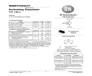
 6 Pages, 190 KB, Original
t may be in either location) *Date Code orientation and/or overbar may vary depending upon manufacturing location. ORDERING INFORMATION Shipping Device Package MMBT4403LT1 SOT-23 3000 Tape & Reel SOT-23 (Pb-Free) 3000 Tape & Reel SOT-23 10,000 Tape & Reel MMBT4403LT1G MMBT4403LT3 MMBT4403LT3G SOT-23 10,000 Tape & Reel (Pb-Free) For information on tape and reel specifications, including part orientation and tape sizes, please refer to our Tape and Reel Packaging Specifications Brochure, BRD8011/D. Preferred devices are recommended choices for future use and best overall value. (c) Semiconductor Components Industries, LLC, 2007 February, 2007 - Rev. 6 1 Publication Order Number: MMBT4403LT1/D MMBT4403LT1 ELECTRICAL CHARACTERISTICS (TA = 25C unless otherwise noted) Characteristic Symbol Min Max Unit OFF CHARACTERISTICS Collector -Emitter Breakdown Voltage (Note 3) (IC = -1.0 mAdc, IB = 0) V(BR)CEO -40 - Vdc Collector -Base Breakdown Voltage (IC = -0.1 mAdc, IE = 0) V(BR)CBO -40 - Vdc Emitter -Base B
 6 Pages, 98 KB, Original


